Quick Summary:

This paper demonstrates the first successful growth of wurtzite III-nitride distributed Bragg reflectors (DBRs) on Si (100) substrates using an AlN/GaN superlattice, achieved through a specific misorientation technique. This breakthrough enables the integration of advanced optical and optoelectronic devices with silicon microelectronics.

Summary

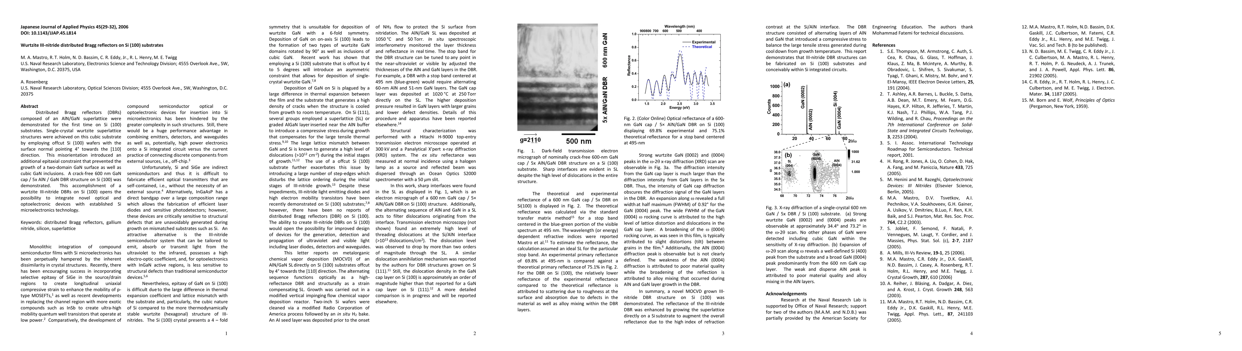
Distributed Bragg reflectors (DBRs) composed of an AlN/GaN superlattice were demonstrated for the first time on Si (100) substrates. Single-crystal wurtzite superlattice structures were achieved on this cubic substrate by employing offcut Si (100) wafers with the surface normal pointing 4{\deg} towards the [110] direction. This misorientation introduced an additional epitaxial constraint that prevented the growth of a two-domain GaN surface as well as cubic GaN inclusions. A crack-free 600 nm GaN cap / 5x AlN / GaN DBR structure on Si (100) was demonstrated. This accomplishment of a wurtzite III-nitride DBRs on Si (100) opens the possibility to integrate novel optical and optoelectronic devices with established Si microelectronics technology.

AI Key Findings

Get AI-generated insights about this paper's methodology, results, and significance.

Paper Details

PDF Preview

Download PDF

Key Terms

gan (0.439)
gan (0.436)
si (0.405)
si (0.385)
cubic (0.253)
cubic (0.251)
demonstrated (0.195)
demonstrated (0.193)
inclusions (0.180)
crack (0.175)
cap (0.172)
surface (0.171)
opens (0.168)
substrates (0.167)
cap (0.167)
substrate (0.165)
surface (0.165)
single crystal (0.162)
deg (0.162)
deg (0.159)
Title Authors Year Actions
Light Output Enhancement of GaN-Based Light-Emitting Diodes Based on AlN/GaN Distributed Bragg Reflectors Grown on Si (111) Substrates
Yibing Yang, Lingxia Zhang, Yu Zhao
2020
View Paper
Nickel Foam as a Substrate for III-nitride Nanowire Growth
M. Mastro, N. Nepal, F. Kub, J. Hite, J. Kim, C. Eddy
2013
View Paper
Characterization of 5 MeV proton-irradiated gallium nitride nanowires
Hyoungjin Kim, Jaehui Ahn, M. Mastro, C. Eddy, J. Han, T. Yang, J. Kim
2009
View Paper
Nature of luminescence and strain in gallium nitride nanowires
M. Mastro, S. Maximenko, M. Gowda, B. Simpkins, P. Pehrsson, J. Long, A. Mäkinen, J. A. Freitas, J. Hite, C. Eddy, J. Kim
2009
View Paper
Characterization of erbium chloride seeded gallium nitride nanocrystals
Jaehui Ahn, M. Mastro, J. Freitas, H.Y. Kim, R. Holm, C. Eddy, J. Hite, S. Maximenko, Jihyun Kim
2008
View Paper
Zinc Sulphide Overlayer Two-Dimensional Photonic Crystal for Enhanced Extraction of Light from a Micro Cavity Light-Emitting Diode
M. Mastro, C. Kim, Mijin Kim, J. Caldwell, R. Holm, I. Vurgaftman, Jihyun Kim, C. Jr., J. Meyer
2008
View Paper
Inductively coupled plasma etching of nano-patterned sapphire for flip-chip GaN light emitting diode applications
Byung Jae Kim, M. Mastro, Hyunjung Jung, H. Kim, S. Kim, R. Holm, J. Hite, C. Eddy, J. Bang, J. Kim
2008
View Paper
Experimental study of plasmonically enhanced GaN nanowire light emitters
M. Mastro, J. Freitas, M. Twigg, R. Holm, C. Eddy, F. Kub, H. Kim, Jaehui Ahn, J. Kim
2008
View Paper
Design of Gallium Nitride Resonant Cavity Light‐Emitting Diodes on Si Substrates
M. Mastro, J. Caldwell, R. Holm, R. Henry, C. Eddy
2008
View Paper
Growth, morphology, and structural properties of group‐III‐nitride nanocolumns and nanodisks
E. Calleja, J. Ristić, S. Fernández-Garrido, L. Cerutti, M. Sánchez-García, J. Grandal, A. Trampert, U. Jahn, G. Sánchez, A. Griol, B. Sánchez
2007
View Paper
Plasmonically enhanced emission from a group-III nitride nanowire emitter
M. Mastro, J. Freitas, O. Glembocki, C. Eddy, R. Holm, R. Henry, J. Caldwell, R. Rendell, F. Kub, J. Kim
2007
View Paper
Rare-earth chloride seeded growth of GaN nano- and micro-crystals
M. Mastro, J. Freitas, R. Holm, C. Eddy, J. Caldwell, K. Liu, O. Glembocki, R. Henry, J. Kim
2007
View Paper
Luminescence characteristics of zinc oxide nanocrystals deposited on glass via a solution method
M. Mastro, J. A. Freitas, C. Eddy, F. Kub, Jaehui Ahn, Hyoungjin Kim, J. Kim
2009
View Paper
Integrated Optics Utilizing GaN-Based Layers on Silicon Substrates
A. Rosenberg, M. Mastro, J. Caldwell, R. Holm, R. Henry, C. Eddy, K. Bussmann, Mijin Kim
2008
View Paper

Comments (0)

This website uses cookies to ensure you get the best experience. Learn more