Atomic-resolution nc-AFM and simultaneous STM/STS measurements were performed on the Si(553)-Au surface under ultrahigh vacuum at 4.3K and 50K using a commercial low-temperature microscope with force-current detection capabilities. DFT calculations were conducted using the Vienna ab initio simulation package with the GGA and PBEsol functional.
Publication
Metrics
AI Quick Summary
This study identifies a Z3 charge density wave (CDW) in atomic chains on Au-decorated vicinal silicon surfaces using atomic force and scanning tunneling microscopy. The chains exhibit a strong buckling pattern forming trimer unitcells, consistent with a rehybridized dangling bond model and ruling out earlier antiferromagnetic spin ordering.
Quick Answers
What is "Z3 Charge Density Wave of Silicon Atomic Chains on a Vicinal Silicon Surface" about?
This study identifies a Z3 charge density wave (CDW) in atomic chains on Au-decorated vicinal silicon surfaces using atomic force and scanning tunneling microscopy. The chains exhibit a strong buckling pattern forming trimer unitcells, consistent with a rehybridized dangling bond model and ruling out earlier antiferromagnetic spin ordering.
What methodology did the authors use?
Atomic-resolution nc-AFM and simultaneous STM/STS measurements were performed on the Si(553)-Au surface under ultrahigh vacuum at 4.3K and 50K using a commercial low-temperature microscope with force-current detection capabilities. DFT calculations were conducted using the Vienna ab initio simulation package with the GGA and PBEsol functional. More in Methodology →
What are the key results?
Strong trimer structural distortion and substantial bandgap along step-edge Si chains at low temperature, corresponding to a CDW ground state and a Z3 topological insulator. — Transient electron doping by tunneling current reduces the stability of the CDW phase, inducing a dynamically fluctuating CDW state at very low temperature. More in Key Results →
Why is this work significant?
This research provides a solid ground for the existence of exotic topological solitons, which could enable topologically-protected multilevel information processing. More in Significance →
What are the main limitations?
Limited to specific surface conditions and materials (Si(553)-Au) — Experimental and theoretical findings may not directly generalize to other 1D systems or different temperature ranges More in Limitations →
Abstract
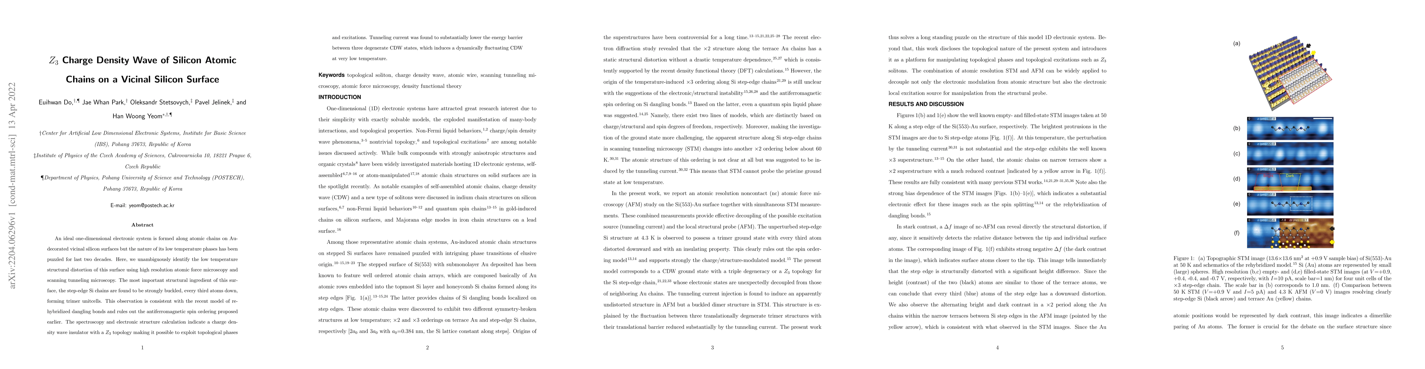
An ideal one-dimensional electronic system is formed along atomic chains on Au-decorated vicinal silicon surfaces but the nature of its low temperature phases has been puzzled for last two decades. Here, we unambiguously identify the low temperature structural distortion of this surface using high resolution atomic force microscopy and scanning tunneling microscopy. The most important structural ingredient of this surface, the step-edge Si chains are found to be strongly buckled, every third atoms down, forming trimer unitcells. This observation is consistent with the recent model of rehybridized dangling bonds and rules out the antiferromagnetic spin ordering proposed earlier. The spectroscopy and electronic structure calculation indicate a charge density wave insulator with a Z3 topology making it possible to exploit topological phases and excitations. Tunneling current was found to substantially lower the energy barrier between three degenerate CDW states, which induces a dynamically fluctuating CDW at very low temperature.
Key Findings, in focus
Seven facets of this paper, analysed and brought into focus by AI.
This research provides a solid ground for the existence of exotic topological solitons, which could enable topologically-protected multilevel information processing.
- Strong trimer structural distortion and substantial bandgap along step-edge Si chains at low temperature, corresponding to a CDW ground state and a Z3 topological insulator.
- Transient electron doping by tunneling current reduces the stability of the CDW phase, inducing a dynamically fluctuating CDW state at very low temperature.
- Three degenerate ground states with a small energy barrier of 13 meV, leading to finite-temperature dynamic fluctuations between them.
This research provides a solid ground for the existence of exotic topological solitons, which could enable topologically-protected multilevel information processing.
Combining atomic-resolution STM and AFM to decouple electronic local excitations from structural probes, revealing the atomic and electronic structure of Si(553)-Au chains.
Unambiguous identification of the low-temperature structural distortion of Si atomic chains on a vicinal silicon surface, revealing a Z3 topological insulator phase and demonstrating dynamic CDW fluctuations induced by electron doping.
- Limited to specific surface conditions and materials (Si(553)-Au)
- Experimental and theoretical findings may not directly generalize to other 1D systems or different temperature ranges
- Investigate topological properties and excitations in this system further
- Explore the potential for topologically-protected multilevel information processing
Impact
Paper Details
Authors
PDF Preview
Citation Network
Current paper (gray), citations (green), references (blue)
Display is limited for performance on very large graphs.
Discussion 0