ZnO-based Semiconductors and Structures for Transistors, Optoelectronic Devices and Sustainable Electronics
Publication
Metrics
AI Quick Summary
This paper reviews the unique properties of zinc oxide-based semiconductors and structures, emphasizing their suitability for transistors, optoelectronic devices, and sustainable electronics due to factors like wide bandgap, high electron mobility, and environmentally-friendly production methods. It discusses how these properties can be tuned for various applications and their role in future sustainable optoelectronics.
Paper Preview
Abstract
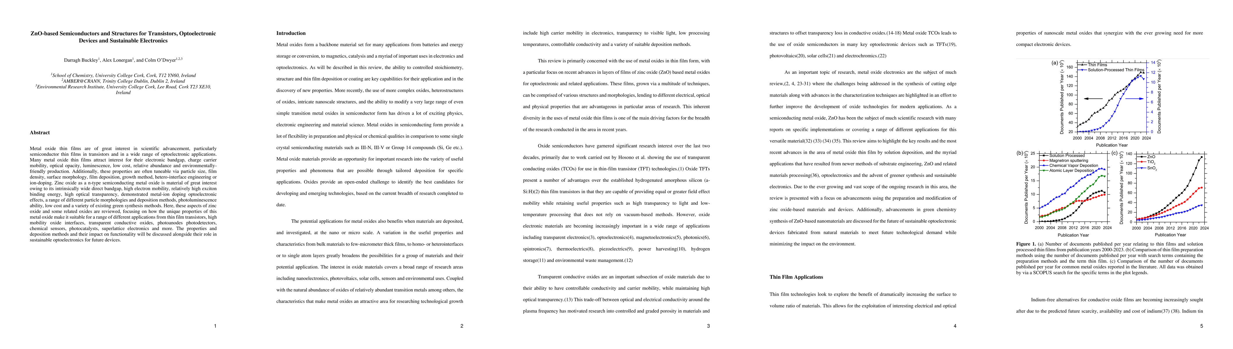
Metal oxide thin films are of great interest in scientific advancement, particularly semiconductor thin films in transistors and in a wide range of optoelectronic applications. Many metal oxide thin films attract interest for their electronic bandgap, charge carrier mobility, optical opacity, luminescence, low cost, relative abundance and environmentally-friendly production. Additionally, these properties are often tuneable via particle size, film density, surface morphology, film deposition, growth method, hetero-interface engineering or ion-doping. Zinc oxide as a n-type semiconducting metal oxide is material of great interest owing to its intrinsically wide direct bandgap, high electron mobility, relatively high exciton binding energy, high optical transparency, demonstrated metal-ion doping optoelectronic effects, a range of different particle morphologies and deposition methods, photoluminescence ability, low cost and a variety of existing green synthesis methods. Here, these aspects of zinc oxide and some related oxides are reviewed, focusing on how the unique properties of this metal oxide make it suitable for a range of different applications from thin film transistors, high mobility oxide interfaces, transparent conductive oxides, photoanodes photodetectors, chemical sensors, photocatalysts, superlattice electronics and more. The properties and deposition methods and their impact on functionality will be discussed alongside their role in sustainable optoelectronics for future devices.
AI Key Findings
Get AI-generated insights about this paper's methodology, results, significance, and more — seven facets brought into focus.
Impact
Paper Details
Authors
PDF Preview
Related Papers
No references found for this paper.
Discussion 0