A Novel Nano Tomography Setup for Material Science and Engineering Applications
Publication
Metrics
Paper Preview
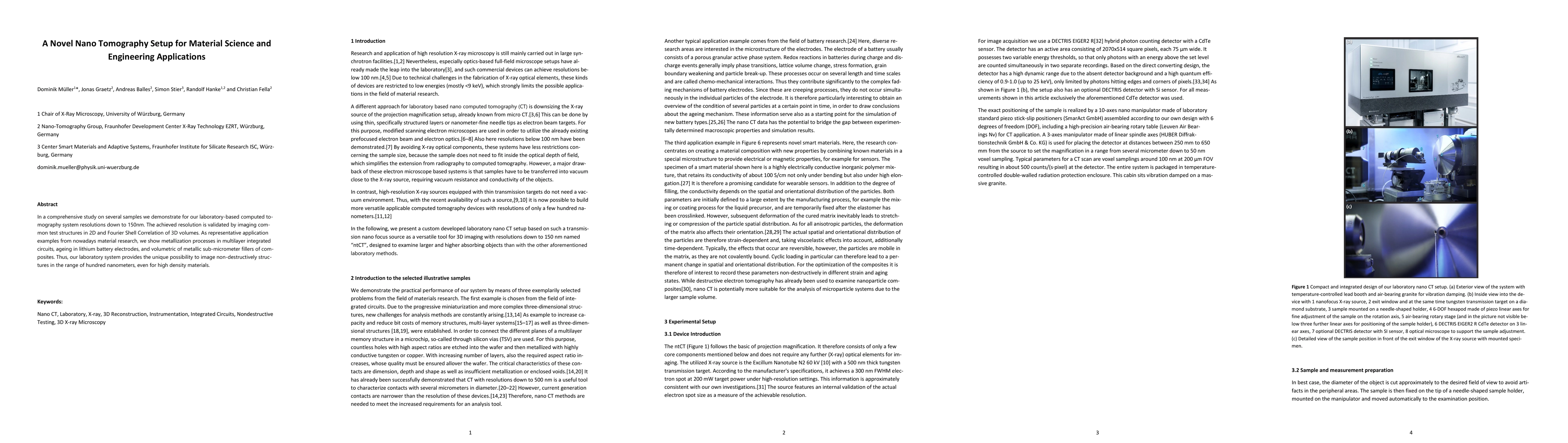
Abstract
In a comprehensive study on several samples we demonstrate for our laboratory-based computed tomography system resolutions down to 150nm. The achieved resolution is validated by imaging com-mon test structures in 2D and Fourier Shell Correlation of 3D volumes. As representative application examples from nowadays material research, we show metallization processes in multilayer integrated circuits, ageing in lithium battery electrodes, and volumetric of metallic sub-micrometer fillers of com-posites. Thus, our laboratory system provides the unique possibility to image non-destructively struc-tures in the range of hundred nanometers, even for high density materials.
AI Key Findings
Get AI-generated insights about this paper's methodology, results, significance, and more — seven facets brought into focus.
Impact
Paper Details
Authors
PDF Preview
Key Terms
Citation Network
Current paper (gray), citations (green), references (blue)
Display is limited for performance on very large graphs.
Discussion 0