The research presents a scalable quadratic nonlinear silicon photonics platform by heterogeneously integrating periodically poled lithium niobate (PPLN) onto a silicon photonics platform, utilizing existing CMOS processes and a generic PPLN design for frequency conversion on two distinct waveguide geometries.
A scalable quadratic nonlinear silicon photonics platform with printable entangled photon-pair sources
Publication
Metrics
AI Quick Summary
This paper presents a scalable quadratic nonlinear silicon photonics platform that integrates periodically poled lithium niobate (PPLN) onto silicon, achieving reproducible phase-matching across a wafer and enabling tunable wavelength conversion. The platform also demonstrates printable entangled photon-pair sources, paving the way for large-scale quantum optical circuits.
Quick Answers
What methodology did the authors use?
The research presents a scalable quadratic nonlinear silicon photonics platform by heterogeneously integrating periodically poled lithium niobate (PPLN) onto a silicon photonics platform, utilizing existing CMOS processes and a generic PPLN design for frequency conversion on two distinct waveguide geometries. More in Methodology →
What are the key results?
Achieved reproducible phase-matching across the full radius of a 200 mm silicon photonics wafer, leveraging superior CMOS fabrication tolerances. — Introduced a tuning mechanism for both blue- and red-shifting of the operating wavelength, enabling deterministic phase-matching over an entire wafer. More in Key Results →
Why is this work significant?
This work represents a significant step towards scalable quadratic nonlinearities, paving the way for their integration into large-scale optical nonlinear systems and facilitating high-volume manufacturing of highly efficient frequency converters. More in Significance →
What are the main limitations?
The study did not explore the long-term stability of the integrated PPLN devices under various environmental conditions. — The research focused on specific wavelength ranges and did not investigate the platform's performance across the entire optical spectrum. More in Limitations →
Abstract
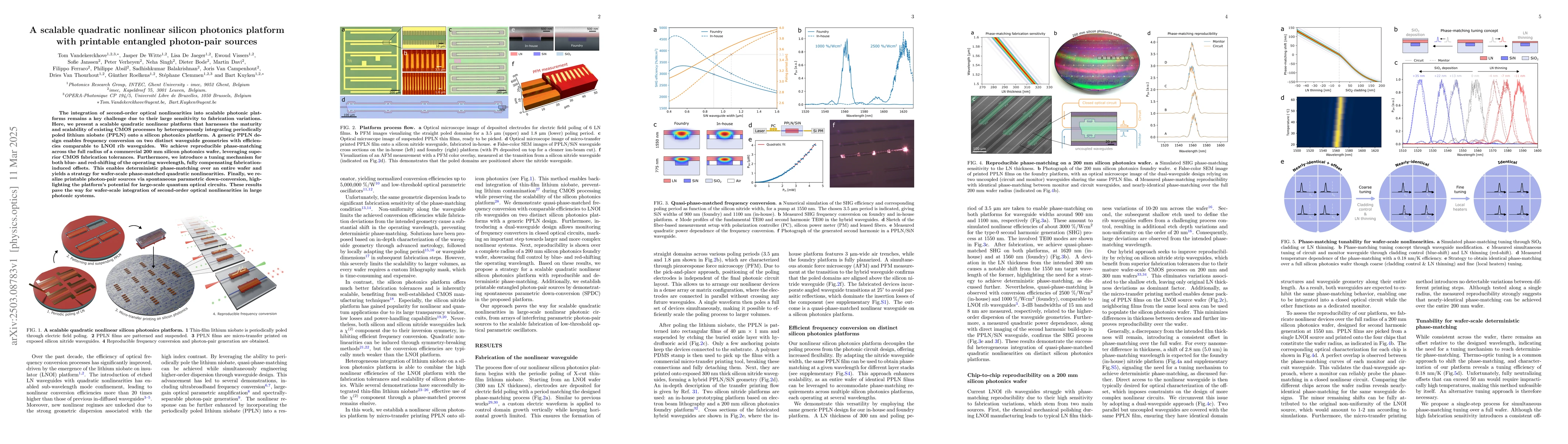
The integration of second-order optical nonlinearities into scalable photonic platforms remains a key challenge due to their large sensitivity to fabrication variations. Here, we present a scalable quadratic nonlinear platform that harnesses the maturity and scalability of existing CMOS processes by heterogeneously integrating periodically poled lithium niobate (PPLN) onto a silicon photonics platform. A generic PPLN design enables frequency conversion on two distinct waveguide geometries with efficiencies comparable to LNOI rib waveguides. We achieve reproducible phase-matching across the full radius of a commercial 200 mm silicon photonics wafer, leveraging superior CMOS fabrication tolerances. Furthermore, we introduce a tuning mechanism for both blue- and red-shifting of the operating wavelength, fully compensating fabrication-induced offsets. This enables deterministic phase-matching over an entire wafer and yields a strategy for wafer-scale phase-matched quadratic nonlinearities. Finally, we realize printable photon-pair sources via spontaneous parametric down-conversion, highlighting the platform's potential for large-scale quantum optical circuits. These results pave the way for wafer-scale integration of second-order optical nonlinearities in large photonic systems.
Key Findings, in focus
Seven facets of this paper, analysed and brought into focus by AI.
This work represents a significant step towards scalable quadratic nonlinearities, paving the way for their integration into large-scale optical nonlinear systems and facilitating high-volume manufacturing of highly efficient frequency converters.
- Achieved reproducible phase-matching across the full radius of a 200 mm silicon photonics wafer, leveraging superior CMOS fabrication tolerances.
- Introduced a tuning mechanism for both blue- and red-shifting of the operating wavelength, enabling deterministic phase-matching over an entire wafer.
- Realized printable photon-pair sources via spontaneous parametric down-conversion, demonstrating the platform's potential for large-scale quantum optical circuits.
This work represents a significant step towards scalable quadratic nonlinearities, paving the way for their integration into large-scale optical nonlinear systems and facilitating high-volume manufacturing of highly efficient frequency converters.
The paper introduces a novel approach for integrating second-order optical nonlinearities into scalable photonic platforms by combining mature CMOS processes with heterogeneous integration of PPLN onto silicon photonics.
The research presents a unique solution to overcome the challenges associated with large sensitivity to fabrication variations in second-order nonlinear platforms, enabling scalability and reproducibility in large photonic systems.
- The study did not explore the long-term stability of the integrated PPLN devices under various environmental conditions.
- The research focused on specific wavelength ranges and did not investigate the platform's performance across the entire optical spectrum.
- Investigate the long-term stability and reliability of the integrated PPLN devices.
- Explore the platform's performance across a broader range of optical wavelengths.
Impact
Paper Details
Authors
PDF Preview
Citation Network
Current paper (gray), citations (green), references (blue)
Display is limited for performance on very large graphs.
Discussion 0