Publication

Published: May 18, 2026
Categories: physics.ins-det, cond-mat.mtrl-sci

Metrics

Source: ArXiv

Quick Actions

View PDF

AI Quick Summary

The study introduces a single Timepix3-based direct electron detector in an SEM with a movable support, enabling all major diffraction geometries (EBSD, RKD, TKD) and imaging modes without hardware changes. This unified detector approach, coupled with optimized acquisition and data processing, allows efficient, multi-type microstructural analysis (including imaging and defect mapping) on both bulk samples and thin foils.

Quick Answers

What is "A single multi-configuration Direct Electron Detector for various electron imaging and diffraction-based techniques in SEM" about?

The study introduces a single Timepix3-based direct electron detector in an SEM with a movable support, enabling all major diffraction geometries (EBSD, RKD, TKD) and imaging modes without hardware changes. This unified detector approach, coupled with optimized acquisition and data processing, allows efficient, multi-type microstructural analysis (including imaging and defect mapping) on both bulk samples and thin foils.

What methodology did the authors use?

Integration of a single Timepix3-based direct electron detector (DED) into an SEM with precise translation and rotation capabilities to realize all principal diffraction geometries (EBSD, RKD, TKD) in on-, off-, and near-axis configurations, accompanied by energy-filtering optimization and a data-driven post-processing approach to reconstruct electron images for BSE, ECCI, and STEM-in-SEM. More in Methodology →

What are the key results?

Demonstrated multi-configuration SEM setup using one DED to perform EBSD, RKD, and TKD across multiple geometries without hardware changes. — Achieved high-quality Kikuchi patterns and dislocations imaging in both reflection and transmission modes across configurations. More in Key Results →

Why is this work significant?

First demonstration of a single Timepix3-based detector enabling integrated multiscale crystallographic and defect analyses in SEM across multiple diffraction geometries, reducing hardware complexity and enabling streamlined workflows for advanced materials characterization. More in Significance →

What are the main limitations?

Reported results limited to specific SEM configurations and may require optimization for different instrument geometries or detectors. — Performance reliance on precise mechanical translation/rotation and energy-filtering settings; potential trade-offs with acquisition speed and data processing load. More in Limitations →

Paper Preview

Abstract

Addressing the need for efficient and integrated multiscale crystallographic and defect analyses of advanced materials, this paper presents the implementation of a new multi-configuration detection system, integrating a single Timepix3-based direct electron detector (DED) in a scanning electron microscope (SEM). By combining precise translation and rotation movements, this system enables, for the first time, the use of the same detector to realize all principal diffraction geometries. These include conventional Electron BackScatter Diffraction (EBSD), off-axis Reflexion Kikuchi Diffraction (RKD), and Transmission Kikuchi Diffraction (TKD) in on-, off- and near-axis configurations. Furthermore, transitions between all these geometries are accomplished without hardware modification. On the other hand, this work presents efficient reconstruction of electron images using the detector data-driven feature, extending thus its applicability to BackScattered Electron imaging (BSE), Electron Channelling Contrast Imaging (ECCI) and Scanning Transmission Electron Imaging in SEM (STEM-in-SEM) characterizations. High-quality Kikuchi patterns easily indexable were acquired across all geometries as well as micrographs of dislocations in both reflection and transmission modes. This is achieved thanks to the flexibility of the implemented detector, the optimizations made in acquisition parameters, such as energy filtering settings, and the efficiency of the developed custom approach used for electron data post-processing. Through this work, it is demonstrated that with a single DED assisted by an orientable support, it is possible to perform multiple advanced microstructural characterizations of both bulk samples and thin foils in the same SEM.
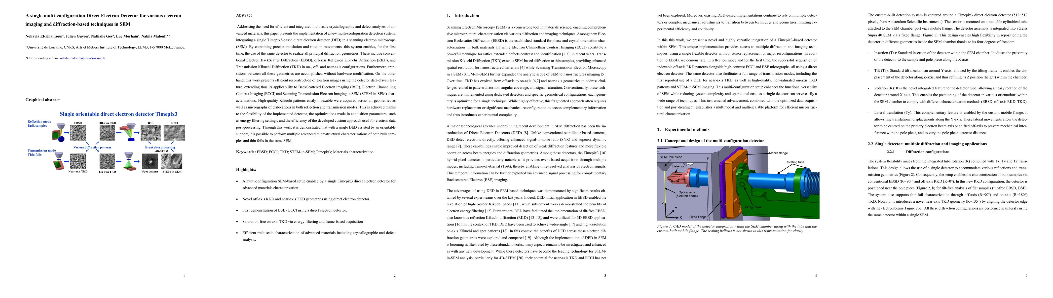
AI Key Findings

Generated May 31, 2026

Methodology — What approach did the authors take?

Integration of a single Timepix3-based direct electron detector (DED) into an SEM with precise translation and rotation capabilities to realize all principal diffraction geometries (EBSD, RKD, TKD) in on-, off-, and near-axis configurations, accompanied by energy-filtering optimization and a data-driven post-processing approach to reconstruct electron images for BSE, ECCI, and STEM-in-SEM.

Key Results — What are the main findings?

  • Demonstrated multi-configuration SEM setup using one DED to perform EBSD, RKD, and TKD across multiple geometries without hardware changes.
  • Achieved high-quality Kikuchi patterns and dislocations imaging in both reflection and transmission modes across configurations.
  • Enabled saturation-free on-axis TKD through energy filtering and frame-based acquisition, with efficient post-processing for data reconstruction.
  • Validated broad applicability to bulk samples and thin foils, enabling concurrent crystallographic and defect analyses within a single SEM.

Significance — Why does this research matter?

First demonstration of a single Timepix3-based detector enabling integrated multiscale crystallographic and defect analyses in SEM across multiple diffraction geometries, reducing hardware complexity and enabling streamlined workflows for advanced materials characterization.

Technical Contribution — What is the technical contribution?

Single DED-enabled multi-configuration SEM platform supporting EBSD, RKD, TKD in multiple axis configurations with energy-filtering optimization and data-driven post-processing for BSE, ECCI, and STEM-in-SEM imaging.

Novelty — What is new about this work?

First integration of a Timepix3 direct electron detector into SEM to realize all principal diffraction geometries with a single orientable detector, enabling seamless transitions between geometries without hardware modification and expanding capabilities to combined crystallography and defect imaging.

Limitations — What are the limitations of this study?

  • Reported results limited to specific SEM configurations and may require optimization for different instrument geometries or detectors.
  • Performance reliance on precise mechanical translation/rotation and energy-filtering settings; potential trade-offs with acquisition speed and data processing load.

Future Work — What did the authors propose for future work?

  • Extend multi-geometry capabilities to additional diffraction modes and higher-throughput 4D-STEM workflows.
  • Develop automated calibration and alignment protocols to generalize the approach across SEM platforms.
  • Refine data-processing algorithms for real-time reconstruction and quantitative dislocation analysis across all geometries.

Paper Details

Paper ID: 2605.18386
Categories:
physics.ins-det cond-mat.mtrl-sci

How to Cite This Paper

BibTeX
@article{guyon2026a,
  title         = {A single multi-configuration Direct Electron Detector for various electron imaging and diffraction-based techniques in SEM},
  author        = {Guyon, Julien and Morhain, Luc and Maloufi, Nabila and others},
  year          = {2026},
  eprint        = {2605.18386},
  archivePrefix = {arXiv},
  primaryClass  = {physics.ins-det},
}
APA 7
Guyon, J., Morhain, L., Maloufi, N., Gey, N., & El-Khairaoui, N. (2026). A single multi-configuration Direct Electron Detector for various electron imaging and diffraction-based techniques in SEM. arXiv. https://arxiv.org/abs/2605.18386
MLA 9
Guyon, Julien, et al. "A single multi-configuration Direct Electron Detector for various electron imaging and diffraction-based techniques in SEM." arXiv, 2026, arxiv.org/abs/2605.18386.

Comments (0)

This website uses cookies to ensure you get the best experience. Learn more