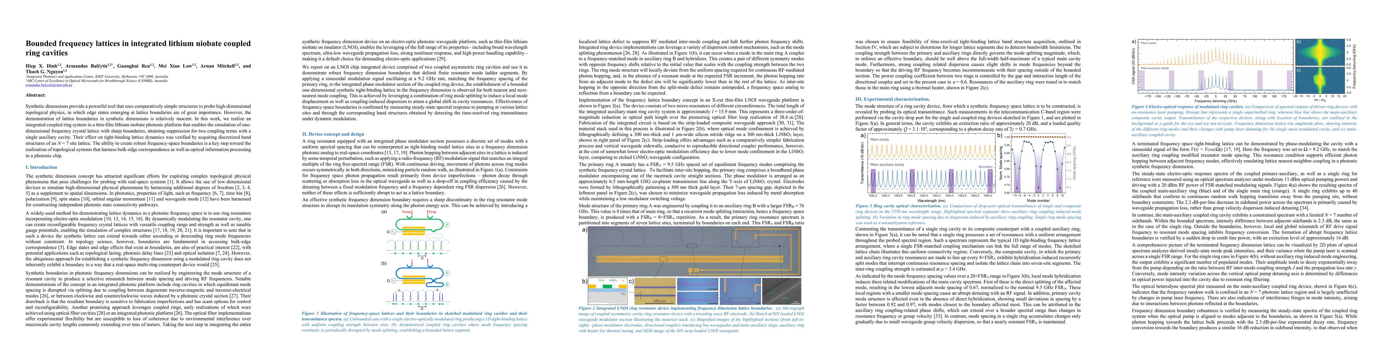
Integrated thin‑film lithium niobate ring resonators with an auxiliary ring were electro‑optically modulated to create a synthetic one‑dimensional frequency lattice; the auxiliary ring’s resonances were thermally tuned to split modes and impose sharp boundaries, and time‑resolved transmittance was measured with a 75 GHz photodetector to obtain band structures.
Bounded frequency lattices in integrated lithium niobate coupled ring cavities
Publication
Metrics
Quick Answers
What methodology did the authors use?
Integrated thin‑film lithium niobate ring resonators with an auxiliary ring were electro‑optically modulated to create a synthetic one‑dimensional frequency lattice; the auxiliary ring’s resonances were thermally tuned to split modes and impose sharp boundaries, and time‑resolved transmittance was measured with a 75 GHz photodetector to obtain band structures. More in Methodology →
What are the key results?
Demonstrated a bounded N = 7 frequency lattice with discrete band‑structure peaks and a measured reflectivity of R ≈ 0.9988. — Showed simultaneous control of nearest‑neighbor (J1 ≈ 0.6 GHz) and next‑nearest‑neighbor (J2 ≈ 0.4 GHz) couplings, enabling observation of both 1×FSR and 2×FSR band structures. More in Key Results →
Why is this work significant?
Provides a scalable, chip‑based platform for engineering topological photonic states and frequency‑comb processing, enabling compact isolation, linear transformations, and quantum walk simulations. More in Significance →
What are the main limitations?
Boundary effectiveness is limited to a few nearest‑neighbor couplings and degrades for higher n×FSR modulation due to mode‑splitting span. — The 7‑site lattice size is constrained by detector bandwidth and fabrication tolerances, limiting exploration of larger synthetic dimensions. More in Limitations →
Abstract
Synthetic dimensions provide a powerful tool that uses comparatively simple structures to probe high-dimensional topological physics, in which edge states emerging at lattice boundaries are of great importance. However, the demonstration of lattice boundaries in synthetic dimensions is relatively nascent. In this work, we realize an integrated coupled ring system in a thin-film lithium niobate photonic platform that enables the simulation of one-dimensional frequency crystal lattice with sharp boundaries, attaining suppression for two coupling terms with a single auxiliary cavity. Their effect on tight-binding lattice dynamics was verified by acquiring discretized band structures of an N = 7 site lattice. The ability to create robust frequency-space boundaries is a key step toward the realization of topological systems that harness bulk-edge correspondence as well as optical information processing in a photonic chip.
Key Findings, in focus
Seven facets of this paper, analysed and brought into focus by AI.
Provides a scalable, chip‑based platform for engineering topological photonic states and frequency‑comb processing, enabling compact isolation, linear transformations, and quantum walk simulations.
- Demonstrated a bounded N = 7 frequency lattice with discrete band‑structure peaks and a measured reflectivity of R ≈ 0.9988.
- Showed simultaneous control of nearest‑neighbor (J1 ≈ 0.6 GHz) and next‑nearest‑neighbor (J2 ≈ 0.4 GHz) couplings, enabling observation of both 1×FSR and 2×FSR band structures.
- Verified that the auxiliary‑ring induced mode splitting suppresses longer‑range coupling and produces a clear 16 dB extinction at the lattice boundaries.
Provides a scalable, chip‑based platform for engineering topological photonic states and frequency‑comb processing, enabling compact isolation, linear transformations, and quantum walk simulations.
Introduced a single auxiliary ring–induced mode‑splitting scheme that creates sharp, tunable frequency‑space boundaries in integrated lithium niobate ring cavities, enabling discrete band‑structure spectroscopy of synthetic lattices.
First on‑chip demonstration of synthetic frequency‑dimension boundaries using a single auxiliary ring, with flexible FSR tuning and simultaneous control of nearest and next‑nearest neighbor couplings, distinct from prior bulk or free‑space implementations.
- Boundary effectiveness is limited to a few nearest‑neighbor couplings and degrades for higher n×FSR modulation due to mode‑splitting span.
- The 7‑site lattice size is constrained by detector bandwidth and fabrication tolerances, limiting exploration of larger synthetic dimensions.
- Optimize cavity coupling and dispersion to extend boundary robustness to larger n×FSR ranges and longer lattices.
- Integrate multiple auxiliary rings or higher‑finesse resonators to suppress even longer‑range couplings and realize higher‑dimensional topological models.
Discussion 0