ArxivLens
ArXiv cond-mat.mes-hall cond-mat.mtrl-sci

Charge transfer between van der Waals coupled metallic 2D layers

Bharti Matta, Craig Polley, Kathrin Küster, Philipp Rosenzweig, Ulrich Starke

2505.07382 Published May 12, 2025
View PDF

Publication

Published: May 12, 2025
Updated: Jun 17, 2025
Categories: cond-mat.mes-hall, cond-mat.mtrl-sci

Metrics

Source: ArXiv

AI Quick Summary

Researchers studied charge transfer in a potassium-adlayer/graphene/lead-monolayer heterostructure, finding that K donates 44% of its electrons to the Pb monolayer and 56% to graphene, not just doping but also inter-layer electron transfer.

Quick Answers

What is "Charge transfer between van der Waals coupled metallic 2D layers" about?

Researchers studied charge transfer in a potassium-adlayer/graphene/lead-monolayer heterostructure, finding that K donates 44% of its electrons to the Pb monolayer and 56% to graphene, not just doping but also inter-layer electron transfer.

What methodology did the authors use?

The study employs synchrotron-based angle-resolved photoemission spectroscopy to analyze the band structure of a potassium-adlayer/graphene/lead-monolayer heterostructure on a SiC substrate, focusing on charge transfer from K to underlying 2D layers. More in Methodology →

What are the key results?

K adsorption leads to significant n-doping of adjacent graphene layer. — Electron transfer occurs from K to the Pb monolayer. More in Key Results →

Why is this work significant?

This research contributes to understanding charge interactions and transfer in van der Waals heterostructures, which is crucial for engineering novel quantum systems with tailored properties. More in Significance →

What are the main limitations?

The study focuses on a specific heterostructure (K/graphene/Pb on SiC), limiting generalizability to other material combinations. — Synchrotron-based angle-resolved photoemission spectroscopy, while powerful, may not capture all subtle charge transfer dynamics. More in Limitations →

Paper Preview

Abstract

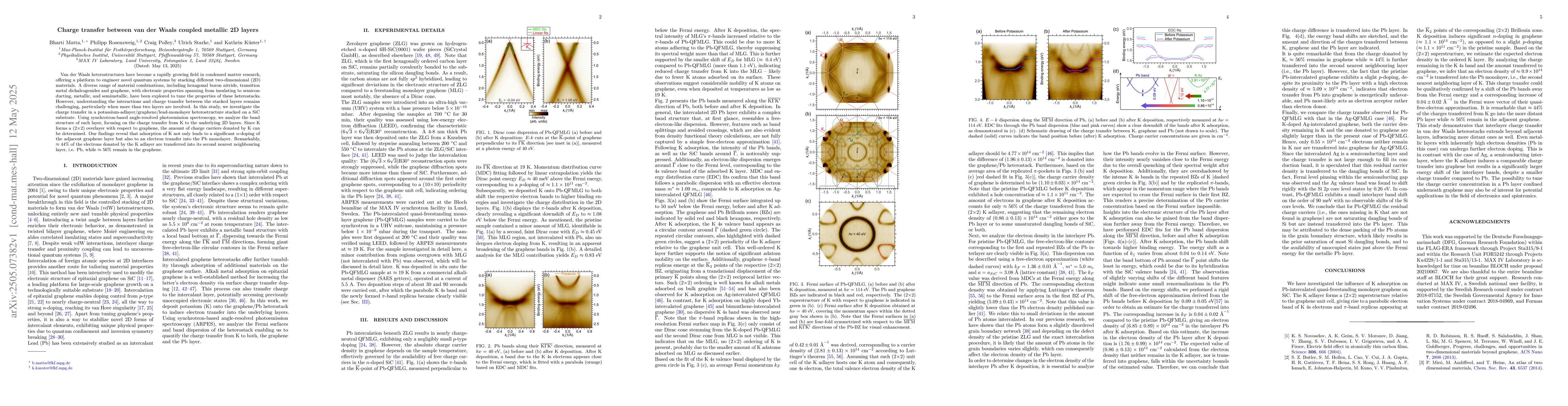
Van der Waals heterostructures have become a rapidly growing field in condensed matter research, offering a platform to engineer novel quantum systems by stacking different two-dimensional (2D) materials. A diverse range of material combinations, including hexagonal boron nitride, transition metal dichalcogenides and graphene, with electronic properties spanning from insulating to semiconducting, metallic, and semimetallic, have been explored to tune the properties of these heterostacks. However, understanding the interactions and charge transfer between the stacked layers remains challenging, particularly when more than two layers are involved. In this study, we investigate the charge transfer in a potassium-adlayer/graphene/lead-monolayer heterostructure stacked on a SiC substrate. Using synchrotron-based angle-resolved photoemission spectroscopy, we analyze the band structure of each layer, focusing on the charge transfer from K to the underlying 2D layers. Since K forms a $(2 \times 2)$ overlayer with respect to graphene, the amount of charge carriers donated by K can be determined. Our findings reveal that adsorption of K not only leads to a significant $n$-doping of the adjacent graphene layer but also to an electron transfer into the Pb monolayer. Remarkably, $\approx 44\%$ of the electrons donated by the K adlayer are transferred into its second nearest neighbouring layer, i.e. Pb, while $\approx 56\%$ remain in the graphene.

Key Findings, in focus

Seven facets of this paper, analysed and brought into focus by AI.

AI-generated · verify against source Generated Jun 08, 2025
In focus · one-line synthesis

This research contributes to understanding charge interactions and transfer in van der Waals heterostructures, which is crucial for engineering novel quantum systems with tailored properties.

01
MethodologyHow they did it

The study employs synchrotron-based angle-resolved photoemission spectroscopy to analyze the band structure of a potassium-adlayer/graphene/lead-monolayer heterostructure on a SiC substrate, focusing on charge transfer from K to underlying 2D layers.

02
ResultsWhat they found
  • K adsorption leads to significant n-doping of adjacent graphene layer.
  • Electron transfer occurs from K to the Pb monolayer.
  • Approximately 44% of electrons donated by K are transferred to Pb, while 56% remain in graphene.
  • K forms a (2×2) overlayer with respect to graphene, facilitating charge transfer quantification.
03
SignificanceWhy it matters

This research contributes to understanding charge interactions and transfer in van der Waals heterostructures, which is crucial for engineering novel quantum systems with tailored properties.

04
Technical ContributionsWhat's new technically

The paper presents a detailed analysis of charge transfer using advanced spectroscopic techniques, providing insights into the behavior of metallic 2D layers in heterostructures.

05
NoveltyWhat sets it apart

The study uniquely quantifies charge transfer between three layers in a van der Waals heterostructure, revealing a significant transfer to the second nearest neighboring layer, which is not commonly observed.

06
LimitationsWhat to be cautious about
  • The study focuses on a specific heterostructure (K/graphene/Pb on SiC), limiting generalizability to other material combinations.
  • Synchrotron-based angle-resolved photoemission spectroscopy, while powerful, may not capture all subtle charge transfer dynamics.
07
Future WorkWhere it goes next
  • Investigate charge transfer in other 2D material combinations within van der Waals heterostructures.
  • Explore charge transfer dynamics under varying environmental conditions, such as temperature and pressure.

Impact

53
References

Paper Details

Paper ID: 2505.07382
Comments: 7 pages, 4 figures
Categories:
cond-mat.mes-hall cond-mat.mtrl-sci

How to Cite This Paper

Reference manager: RIS EndNote

Citation Network

Current paper (gray), citations (green), references (blue)

Display is limited for performance on very large graphs.

Current Paper
Citations
References
Click to view


Discussion 0

This website uses cookies to ensure you get the best experience. Learn more