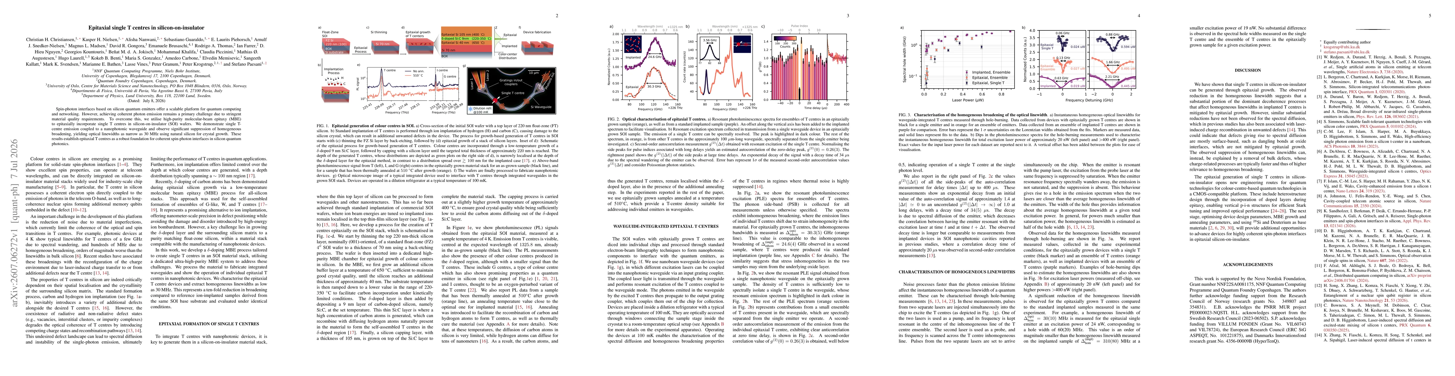
The study develops a δ-doped MBE process to epitaxially incorporate single T centers in a silicon-on-insulator stack. This involves thinning a float-zone SOI wafer to 70 nm, growing a silicon buffer (~40 nm) at high temperature, reducing substrate temperature to 220–350 °C to form a δ-doped Si:C layer (9 nm) for T-centre formation, and capping with ~105 nm silicon before higher-temperature growth to ensure crystal quality. The epitaxial stack is then processed to fabricate nanophotonic waveguides and integrated devices, with optical characterization performed at ≲100 mK to demonstrate single-T-centre emission coupled to the waveguide and linewidth measurements down to 30 MHz, along with spectral-hole-burning and second-order correlation measurements to verify coherence and single-photon emission.
Publication
Metrics
AI Quick Summary
Researchers used high-purity molecular-beam epitaxy to embed a single T center into silicon-on-insulator wafers. They demonstrated emission of a single T center coupled to a nanophotonic waveguide with very narrow optical linewidths (as low as 30 MHz), showing a path toward coherent spin-photon interfaces in silicon quantum photonics.
Quick Answers
What is "Epitaxial single T centres in silicon-on-insulator" about?
Researchers used high-purity molecular-beam epitaxy to embed a single T center into silicon-on-insulator wafers. They demonstrated emission of a single T center coupled to a nanophotonic waveguide with very narrow optical linewidths (as low as 30 MHz), showing a path toward coherent spin-photon interfaces in silicon quantum photonics.
What methodology did the authors use?
The study develops a δ-doped MBE process to epitaxially incorporate single T centers in a silicon-on-insulator stack. This involves thinning a float-zone SOI wafer to 70 nm, growing a silicon buffer (~40 nm) at high temperature, reducing substrate temperature to 220–350 °C to form a δ-doped Si:C layer (9 nm) for T-centre formation, and capping with ~105 nm silicon before... More in Methodology →
What are the key results?
Single T-centre emission coupled to an integrated nanophotonic waveguide was demonstrated in epitaxially grown SOI, confirming successful device integration. — Optical linewidths as narrow as 30 MHz were observed at 4 K, representing a significant suppression of homogeneous broadening compared to implanted references. More in Key Results →
Why is this work significant?
Demonstrates a scalable epitaxial route to integrate coherent T-centres with nanophotonic devices on silicon-on-insulator, enabling robust spin-photon interfaces in silicon quantum photonics and advancing toward scalable quantum networks and processors. More in Significance →
What are the main limitations?
Current work focuses on a single T-centre demonstration; scalability to large-area, uniform arrays remains to be established. — Presence of ancillary colour centres (G and I) in the δ-doped region may complicate spectral filtering and indistinguishability. More in Limitations →
Paper Preview
Abstract
Spin-photon interfaces based on silicon quantum emitters offer a scalable platform for quantum computing and networking. However, achieving coherent photon emission remains a primary challenge due to stringent material quality requirements. To overcome this, we utilise high-purity molecular-beam epitaxy (MBE) to epitaxially incorporate single T centres in silicon-on-insulator (SOI) wafers. We demonstrate single T-centre emission coupled to a nanophotonic waveguide and observe significant suppression of homogeneous broadening, yielding optical linewidths as narrow as 30 MHz using natural silicon for crystal growth. These results establish epitaxial T centres as a robust foundation for coherent spin-photon interfaces in silicon quantum photonics.
Key Findings, in focus
Seven facets of this paper, analysed and brought into focus by AI.
Demonstrates a scalable epitaxial route to integrate coherent T-centres with nanophotonic devices on silicon-on-insulator, enabling robust spin-photon interfaces in silicon quantum photonics and advancing toward scalable quantum networks and processors.
- Single T-centre emission coupled to an integrated nanophotonic waveguide was demonstrated in epitaxially grown SOI, confirming successful device integration.
- Optical linewidths as narrow as 30 MHz were observed at 4 K, representing a significant suppression of homogeneous broadening compared to implanted references.
- Emission spectra show T-centre signals at 1325.8 nm with ancillary G and I centres present in the δ-doped region, indicating successful formation and selective incorporation of the T centres.
- Spectral-hole-burning and time-correlated measurements validate coherent spin-photon interfaces and enable characterization of optical coherence at millikelvin temperatures.
- Annealing tests suggest robustness of grown emitters to high-temperature processing, with comparable behavior to implanted samples under identical conditions.
Demonstrates a scalable epitaxial route to integrate coherent T-centres with nanophotonic devices on silicon-on-insulator, enabling robust spin-photon interfaces in silicon quantum photonics and advancing toward scalable quantum networks and processors.
A dedicated ultra-high-purity MBE process enabling δ-doped epitaxial growth of single T-centres in SOI, integrated with nanophotonic waveguides, achieving few tens of MHz optical linewidths and coherent spin-photon interface capabilities in silicon quantum photonics.
First demonstration of epitaxial growth of single T centres in silicon-on-insulator with integrated nanophotonic devices, achieving narrow homogeneous linewidths and coherent emission via a δ-doping MBE approach that avoids damage from ion implantation.
- Current work focuses on a single T-centre demonstration; scalability to large-area, uniform arrays remains to be established.
- Presence of ancillary colour centres (G and I) in the δ-doped region may complicate spectral filtering and indistinguishability.
- Long-term stability and reproducibility across wafers and fabrication runs require further systematic study.
- Develop tighter spectral filtering and fabrication controls to purify T-centre emission and minimize nearby defect contributions.
- Explore deterministic positioning strategies to place individual T-centres at predefined nanophotonic mode maxima for enhanced photon indistinguishability.
- Scale the epitaxial process to wafer-scale production and quantify device yield, uniformity, and integration with more complex photonic circuits.
Discussion 0