01
MethodologyHow they did it
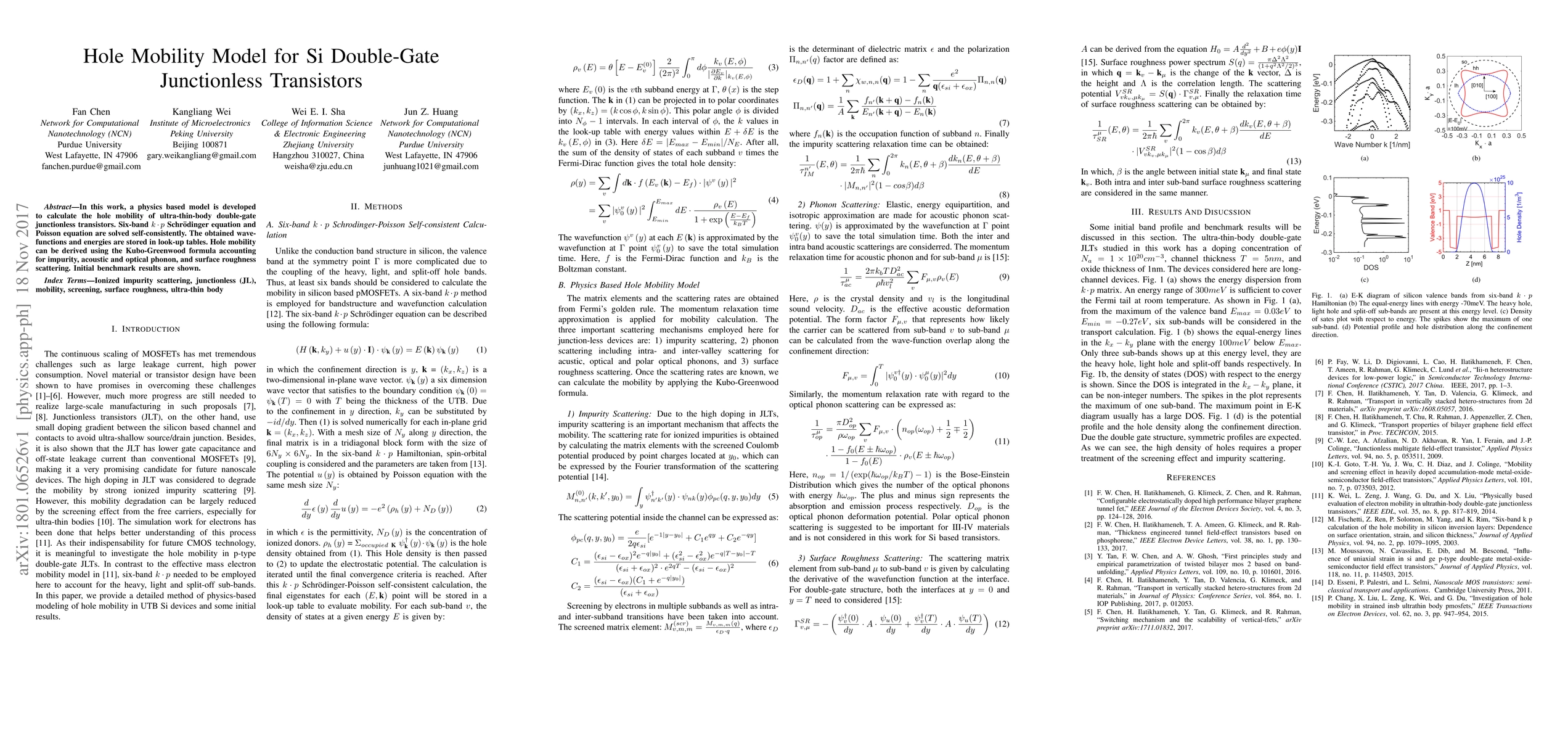
A physics-based model is developed to calculate hole mobility in ultra-thin-body double-gate junctionless transistors by solving six-band k·p Schrödinger and Poisson equations self-consistently. The wave-functions and energies are stored in look-up tables for mobility derivation using the Kubo-Greenwood formula, accounting for impurity, acoustic and optical phonon, and surface roughness scattering.
Discussion 0