ArxivLens

Publication

Published: Mar 02, 2026
Categories: cond-mat.mes-hall

Metrics

Source: ArXiv

Quick Answers

What methodology did the authors use?

Scanning tunneling spectroscopy at 4.2 K on cleaved black phosphorus surfaces, measuring dI/dV spectra while varying tip–sample separation and bias to probe tip‑induced electric fields; data interpreted with a simplified model of a field‑dependent Gaussian surface resonance peak coupled to bulk bands More in Methodology →

What are the key results?

Surface resonance states near the valence‑band edge dominate the screening of a strong external electric field, producing a pronounced conductance dip whose position shifts continuously with the local field — Bulk band edges remain pinned, indicating efficient surface screening and negligible bulk band bending despite the strong tip‑induced field More in Key Results →

Why is this work significant?

The work demonstrates that surface‑localized resonance states can control electrostatic screening and tunneling transport in semiconductors, implying that device designs must account for such states even on clean surfaces; this insight is crucial for nanoscale transistor and sensor technologies More in Significance →

What are the main limitations?

The simplified model neglects self‑consistent Poisson–Schrödinger calculations and detailed band structure of the resonance — Experimental data are not publicly available, limiting independent verification More in Limitations →

Paper Preview

Abstract

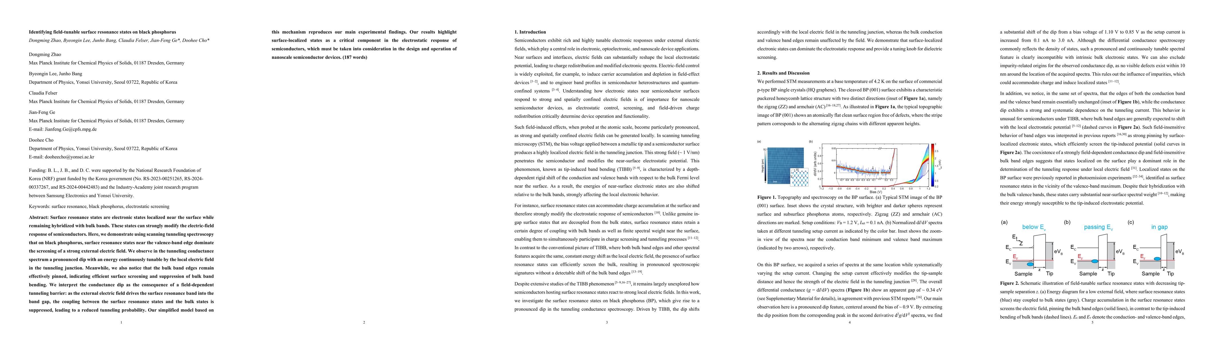
Surface resonance states are electronic states localized near the surface while remaining hybridized with bulk bands. These states can strongly modify the electric-field response of semiconductors. Here, we demonstrate using scanning tunneling spectroscopy that on black phosphorus, surface resonance states near the valence-band edge dominate the screening of a strong external electric field. We observe in the tunneling conductance spectrum a pronounced dip with an energy continuously tunable by the local electric field in the tunneling junction. Meanwhile, we also notice that the bulk band edges remain effectively pinned, indicating efficient surface screening and suppression of bulk band bending. We interpret the conductance dip as the consequence of a field-dependent tunneling barrier: as the external electric field drives the surface resonance band into the band gap, the coupling between the surface resonance states and the bulk states is suppressed, leading to a reduced tunneling probability. Our simplified model based on this mechanism reproduces our main experimental findings. Our results highlight surface-localized states as a critical component in the electrostatic response of semiconductors, which must be taken into consideration in the design and operation of nanoscale semiconductor devices.

Key Findings, in focus

Seven facets of this paper, analysed and brought into focus by AI.

AI-generated · verify against source Generated Mar 03, 2026
In focus · one-line synthesis

The work demonstrates that surface‑localized resonance states can control electrostatic screening and tunneling transport in semiconductors, implying that device designs must account for such states even on clean surfaces; this insight is crucial for nanoscale transistor and sensor technologies

01
MethodologyHow they did it

Scanning tunneling spectroscopy at 4.2 K on cleaved black phosphorus surfaces, measuring dI/dV spectra while varying tip–sample separation and bias to probe tip‑induced electric fields; data interpreted with a simplified model of a field‑dependent Gaussian surface resonance peak coupled to bulk bands

02
ResultsWhat they found
  • Surface resonance states near the valence‑band edge dominate the screening of a strong external electric field, producing a pronounced conductance dip whose position shifts continuously with the local field
  • Bulk band edges remain pinned, indicating efficient surface screening and negligible bulk band bending despite the strong tip‑induced field
  • A simplified model that treats the surface resonance as a moving Gaussian peak reproduces the dip position and its dependence on tip–sample distance, confirming that the dip arises from reduced tunneling probability when the resonance enters the band gap
03
SignificanceWhy it matters

The work demonstrates that surface‑localized resonance states can control electrostatic screening and tunneling transport in semiconductors, implying that device designs must account for such states even on clean surfaces; this insight is crucial for nanoscale transistor and sensor technologies

04
Technical ContributionsWhat's new technically

First experimental observation and quantitative modeling of field‑tunable surface resonance states on black phosphorus, linking their field‑driven shift into the band gap to a measurable conductance dip in STS

05
NoveltyWhat sets it apart

Unlike prior studies that focused on defect states, this work shows that intrinsic surface resonance states can dominate electrostatic response and tunneling transport, revealing a new mechanism for screening in clean semiconductor surfaces

06
LimitationsWhat to be cautious about
  • The simplified model neglects self‑consistent Poisson–Schrödinger calculations and detailed band structure of the resonance
  • Experimental data are not publicly available, limiting independent verification
07
Future WorkWhere it goes next
  • Develop self‑consistent theoretical treatments of surface resonance states under tip‑induced fields
  • Extend the study to other 2D and bulk semiconductors to assess the generality of surface‑resonance‑driven screening

Paper Details

Paper ID: 2603.01848
Categories:
cond-mat.mes-hall

How to Cite This Paper

Reference manager: RIS EndNote


Discussion 0

This website uses cookies to ensure you get the best experience. Learn more