Publication
Metrics
AI Quick Summary
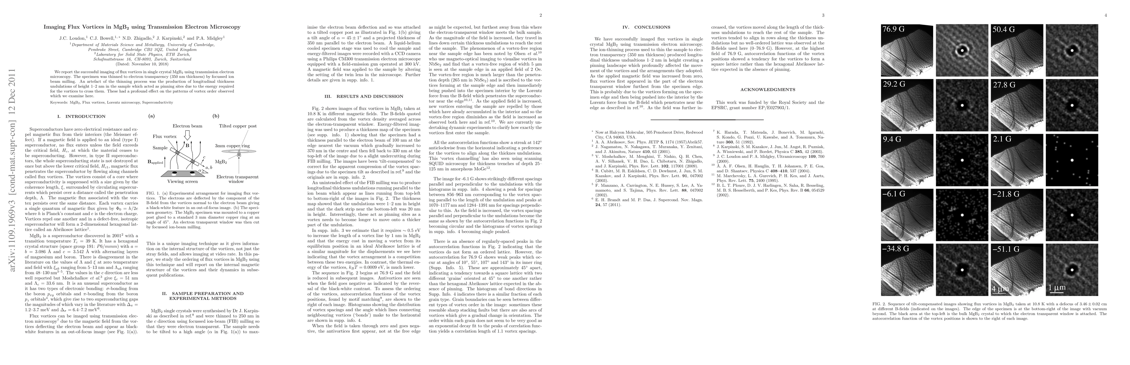
This study successfully images flux vortices in MgB2 using transmission electron microscopy, revealing how thinning-induced thickness undulations act as pinning sites affecting vortex patterns. The research provides insights into vortex dynamics and pinning mechanisms in superconducting materials.
Paper Preview
Abstract
We report the successful imaging of flux vortices in single crystal MgB2 using transmission electron microscopy. The specimen was thinned to electron transparency (350 nm thickness) by focussed ion beam milling. An artefact of the thinning process was the production of longitudinal thickness undulations of height 1-2 nm in the sample which acted as pinning sites due to the energy required for the vortices to cross them. These had a profound effect on the patterns of vortex order observed which we examine here. Supplementary information can be downloaded from http://www-hrem.msm.cam.ac.uk/people/loudon/#publications
AI Key Findings
Get AI-generated insights about this paper's methodology, results, significance, and more — seven facets brought into focus.
Impact
Paper Details
PDF Preview
Key Terms
Citation Network
Current paper (gray), citations (green), references (blue)
Display is limited for performance on very large graphs.
Discussion 0