ArxivLens
ArXiv physics.optics

Inverse design for scalable photonic systems

Geun Ho Ahn, Jelena Vučković, Louise Schul, Sungjun Eun, Sydney Mason

2602.18666 Published Feb 21, 2026
View PDF

Publication

Published: Feb 21, 2026
Categories: physics.optics

Metrics

Source: ArXiv

Quick Answers

What methodology did the authors use?

Review of recent progress in large-scale 3D inverse design, fabrication-aware and robust optimization, translation to commercial foundries, and extension to diverse materials and wavelengths, with synthesis of key challenges and future directions More in Methodology →

What are the key results?

Demonstrated scalable inverse-designed devices achieving 1.12 Tb/s data transmission and 4‑channel CWDM demultiplexers with sub‑dB insertion loss — Introduced fabrication‑aware and robust inverse design that reduces sensitivity to process variations, enabling reliable commercial foundry integration More in Key Results →

Why is this work significant?

Provides a comprehensive roadmap for deploying inverse design in industry, enabling compact, high‑performance photonic components for optical interconnects, quantum photonics, and emerging THz technologies, thereby accelerating the transition from laboratory prototypes to commercial products More in Significance →

What are the main limitations?

High computational cost and memory demands for large 3‑D designs limit scalability — Residual fabrication constraints still restrict achievable feature sizes and introduce variability that can degrade performance More in Limitations →

Paper Preview

Abstract

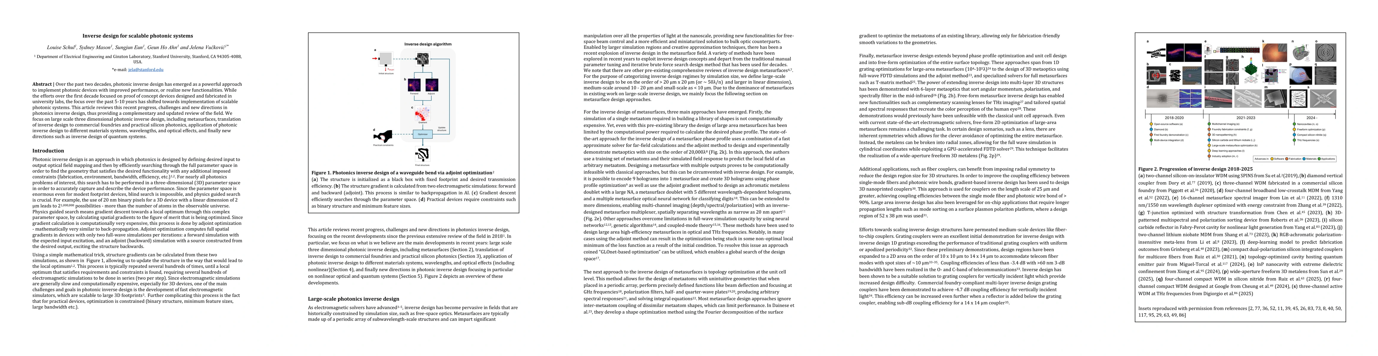
Over the past two decades, photonic inverse design has emerged as a powerful approach to implement photonic devices with improved performance, or realize new functionalities. While the efforts over the first decade focused on proof of concept devices designed and fabricated in university labs, the focus over the past 5-10 years has shifted towards implementation of scalable photonic systems. This article reviews this recent progress, challenges and new directions in photonics inverse design, thus providing a complementary and updated review of the field. We focus on large scale three dimensional photonic inverse design, including metasurfaces, translation of inverse design to commercial foundries and practical silicon photonics, application of photonic inverse design to different materials systems, wavelengths, and optical effects, and finally new directions such as inverse design of quantum systems.

Key Findings, in focus

Seven facets of this paper, analysed and brought into focus by AI.

AI-generated · verify against source Generated Feb 24, 2026
In focus · one-line synthesis

Provides a comprehensive roadmap for deploying inverse design in industry, enabling compact, high‑performance photonic components for optical interconnects, quantum photonics, and emerging THz technologies, thereby accelerating the transition from laboratory prototypes to commercial products

01
MethodologyHow they did it

Review of recent progress in large-scale 3D inverse design, fabrication-aware and robust optimization, translation to commercial foundries, and extension to diverse materials and wavelengths, with synthesis of key challenges and future directions

02
ResultsWhat they found
  • Demonstrated scalable inverse-designed devices achieving 1.12 Tb/s data transmission and 4‑channel CWDM demultiplexers with sub‑dB insertion loss
  • Introduced fabrication‑aware and robust inverse design that reduces sensitivity to process variations, enabling reliable commercial foundry integration
  • Extended inverse design to silicon nitride, lithium niobate, diamond, silicon carbide, hBN, and THz/microwave regimes, showing versatility across materials and wavelengths
03
SignificanceWhy it matters

Provides a comprehensive roadmap for deploying inverse design in industry, enabling compact, high‑performance photonic components for optical interconnects, quantum photonics, and emerging THz technologies, thereby accelerating the transition from laboratory prototypes to commercial products

04
Technical ContributionsWhat's new technically

Systematic synthesis of fabrication‑aware, robust, and multi‑material inverse‑design methodologies, highlighting their application to scalable photonic systems and quantum devices, and outlining a roadmap for industry adoption

05
NoveltyWhat sets it apart

First comprehensive review that collates scalable inverse‑design achievements across multiple materials, wavelengths, and quantum platforms, offering a unified framework and actionable guidance for bridging academia and industry

06
LimitationsWhat to be cautious about
  • High computational cost and memory demands for large 3‑D designs limit scalability
  • Residual fabrication constraints still restrict achievable feature sizes and introduce variability that can degrade performance
07
Future WorkWhere it goes next
  • Integrate AI tools for structure initialization and objective function definition to reduce trial‑and‑error
  • Develop stricter computational bounds and more powerful simulators to enable design of full‑system photonic chips

Paper Details

Paper ID: 2602.18666
Comments: 22 pages, 4 figures
Categories:
physics.optics

How to Cite This Paper

Reference manager: RIS EndNote


Discussion 0

This website uses cookies to ensure you get the best experience. Learn more