Large-scale defects hidden inside a topological insulator grown onto a 2D substrate
Publication
Metrics
Paper Preview
Abstract
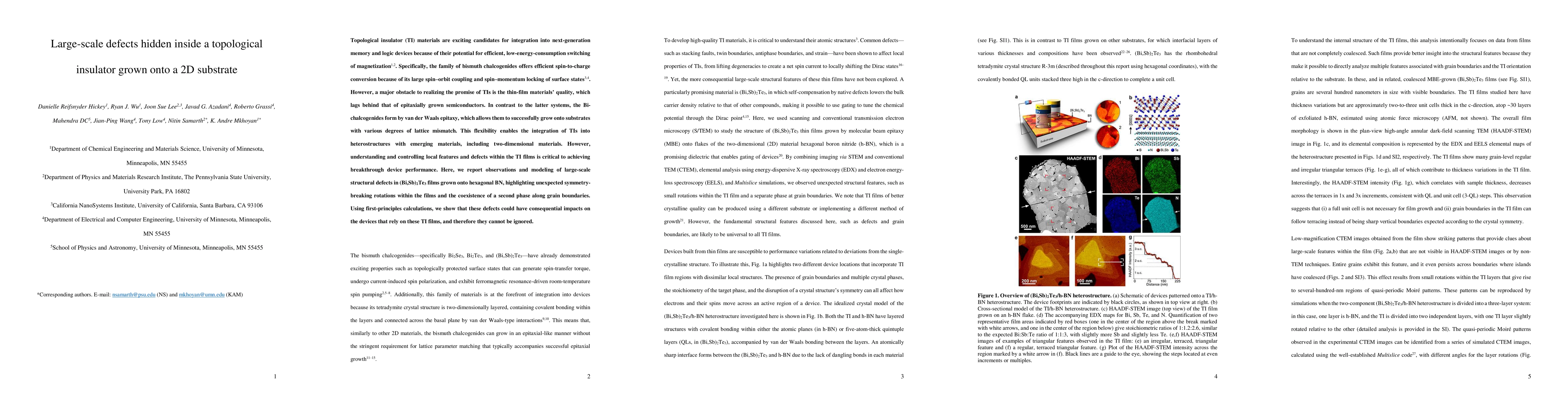
Topological insulator (TI) materials are exciting candidates for integration into next-generation memory and logic devices because of their potential for efficient, low-energy-consumption switching of magnetization. Specifically, the family of bismuth chalcogenides offers efficient spin-to-charge conversion because of its large spin-orbit coupling and spin-momentum locking of surface states. However, a major obstacle to realizing the promise of TIs is the thin-film materials' quality, which lags behind that of epitaxially grown semiconductors. In contrast to the latter systems, the Bi-chalcogenides form by van der Waals epitaxy, which allows them to successfully grow onto substrates with various degrees of lattice mismatch. This flexibility enables the integration of TIs into heterostructures with emerging materials, including two-dimensional materials. However, understanding and controlling local features and defects within the TI films is critical to achieving breakthrough device performance. Here, we report observations and modeling of large-scale structural defects in (Bi,Sb)$_2$Te$_3$ films grown onto hexagonal BN, highlighting unexpected symmetry-breaking rotations within the films and the coexistence of a second phase along grain boundaries. Using first-principles calculations, we show that these defects could have consequential impacts on the devices that rely on these TI films, and therefore they cannot be ignored.
AI Key Findings
Get AI-generated insights about this paper's methodology, results, significance, and more — seven facets brought into focus.
Impact
Paper Details
Authors
PDF Preview
Key Terms
Citation Network
Current paper (gray), citations (green), references (blue)
Display is limited for performance on very large graphs.
Discussion 0