Laser-cut Patterned, Micrometer-thin Diamond Membranes with Coherent Color Centers for Open Microcavities
Publication
Metrics
Paper Preview
Abstract
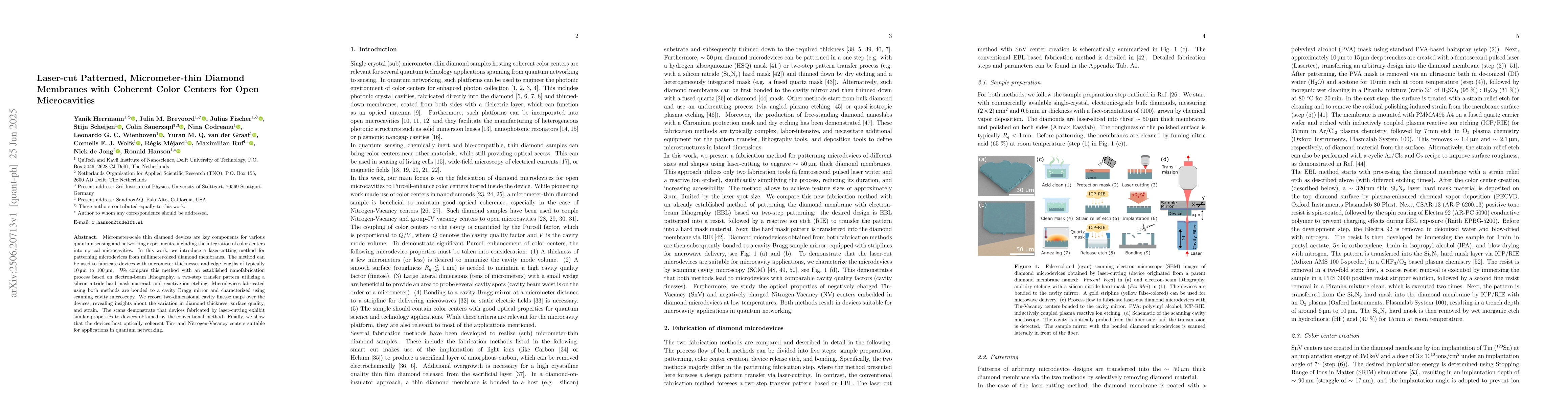
Micrometer-scale thin diamond devices are key components for various quantum sensing and networking experiments, including the integration of color centers into optical microcavities. In this work, we introduce a laser-cutting method for patterning microdevices from millimeter-sized diamond membranes. The method can be used to fabricate devices with micrometer thicknesses and edge lengths of typically 10 $\mu m$ to 100 $\mu m$. We compare this method with an established nanofabrication process based on electron-beam lithography, a two-step transfer pattern utilizing a silicon nitride hard mask material, and reactive ion etching. Microdevices fabricated using both methods are bonded to a cavity Bragg mirror and characterized using scanning cavity microscopy. We record two-dimensional cavity finesse maps over the devices, revealing insights about the variation in diamond thickness, surface quality, and strain. The scans demonstrate that devices fabricated by laser-cutting exhibit similar properties to devices obtained by the conventional method. Finally, we show that the devices host optically coherent Tin- and Nitrogen-Vacancy centers suitable for applications in quantum networking.
AI Key Findings
Get AI-generated insights about this paper's methodology, results, significance, and more — seven facets brought into focus.
Impact
Paper Details
Authors
PDF Preview
Citation Network
Current paper (gray), citations (green), references (blue)
Display is limited for performance on very large graphs.
Discussion 0