Laser-written scalable sapphire integrated photonics platform
Publication
Metrics
AI Quick Summary
This paper showcases laser-written sapphire photonic devices, integrating multi-layer waveguides at 780 nm and 1550 nm with low propagation losses, and demonstrates scalable fabrication of various photonic structures using femtosecond laser direct writing. The work opens avenues for applications in communications, imaging, computing, and sensing.
Paper Preview
Abstract
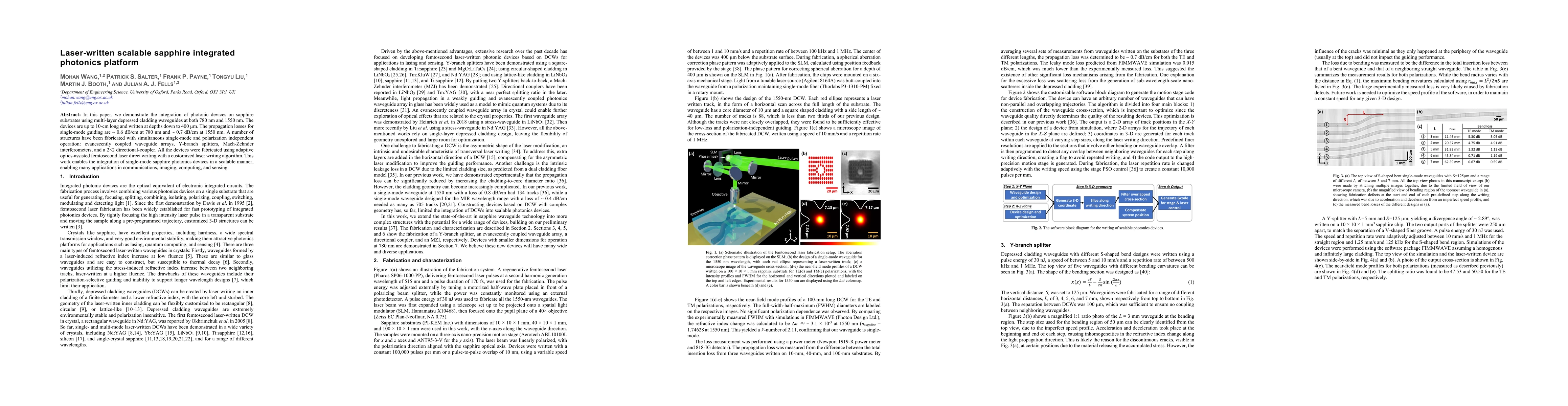
In this paper, we demonstrate the integration of photonic devices on sapphire substrates using multi-layer depressed cladding waveguides at both 780 nm and 1550 nm. The devices are up to 10-cm long and written at depths down to 400 um. The propagation losses for single-mode guiding are ~ 0.6 dB/cm at 780 nm and ~ 0.7 dB/cm at 1550 nm. A number of structures have been fabricated with simultaneous single-mode and polarization independent operation: evanescently coupled waveguide arrays, Y-branch splitters, Mach-Zehnder interferometers, and a 2x2 directional-coupler. All the devices were fabricated using adaptive optics-assisted femtosecond laser direct writing with a customized laser writing algorithm. This work enables the integration of single-mode sapphire photonics devices in a scalable manner, enabling many applications in communications, imaging, computing, and sensing.
AI Key Findings
Get AI-generated insights about this paper's methodology, results, significance, and more — seven facets brought into focus.
Impact
Authors
PDF Preview
Citation Network
Current paper (gray), citations (green), references (blue)
Display is limited for performance on very large graphs.
Discussion 0