Publication
Metrics
AI Quick Summary
This paper demonstrates on-chip detection of carrier-envelope-phase (CEP) using optical-field-driven photocurrents in a scalable, monolithic array of plasmonic nanoantennas. The technique requires significantly less pulse energy compared to ionization-based methods, paving the way for compact, integrated circuits in petahertz electronics and attosecond science.
Paper Preview
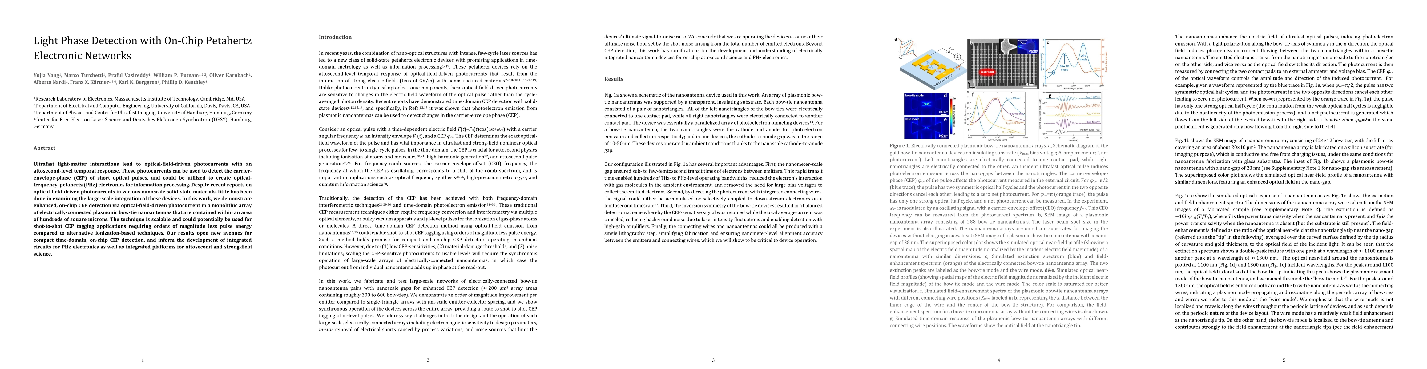
Abstract
Ultrafast light-matter interactions lead to optical-field-driven photocurrents with an attosecond-level temporal response. These photocurrents can be used to detect the carrier-envelope-phase (CEP) of short optical pulses, and could be utilized to create optical-frequency, petahertz (PHz) electronics for information processing. Despite recent reports on optical-field-driven photocurrents in various nanoscale solid-state materials, little has been done in examining the large-scale integration of these devices. In this work, we demonstrate enhanced, on-chip CEP detection via optical-field-driven photocurrent in a monolithic array of electrically-connected plasmonic bow-tie nanoantennas that are contained within an area of hundreds of square microns. The technique is scalable and could potentially be used for shot-to-shot CEP tagging applications requiring orders of magnitude less pulse energy compared to alternative ionization-based techniques. Our results open new avenues for compact time-domain, on-chip CEP detection, and inform the development of integrated circuits for PHz electronics as well as integrated platforms for attosecond and strong-field science.
AI Key Findings
Get AI-generated insights about this paper's methodology, results, significance, and more — seven facets brought into focus.
Impact
Paper Details
Authors
PDF Preview
Key Terms
Citation Network
Current paper (gray), citations (green), references (blue)
Display is limited for performance on very large graphs.
Discussion 0