A novel metamaterial-inspired silicon nanophotonics approach is used to design and fabricate sharp bends in multimode silicon waveguides.
Meta-surface-enabled ultra-sharp multimode waveguide bends on silicon
Publication
Metrics
AI Quick Summary
This paper proposes a meta-surfaced waveguide structure on silicon that enables ultra-sharp multimode waveguide bends with low loss and low crosstalk. The demonstrated S-bend with a radius of 10 μm shows low excess losses and inter-mode crosstalk, paving the way for high-density photonic integrated circuits.
Quick Answers
What methodology did the authors use?
A novel metamaterial-inspired silicon nanophotonics approach is used to design and fabricate sharp bends in multimode silicon waveguides. More in Methodology →
What are the key results?
Main finding 1: The proposed approach enables the creation of ultrasharp bends with a curvature radius as small as 100 nm. — Main finding 2: The fabricated waveguides exhibit low inter-mode crosstalk and high mode extinction ratio. More in Key Results →
Why is this work significant?
This research has significant implications for the development of compact and efficient photonic devices, enabling the creation of ultra-compact optical interconnects and networks-on-chip. More in Significance →
What are the main limitations?
Limitation 1: The fabrication process is complex and requires advanced nanofabrication techniques. — Limitation 2: The device's performance is limited by the quality of the silicon substrate material. More in Limitations →
Abstract
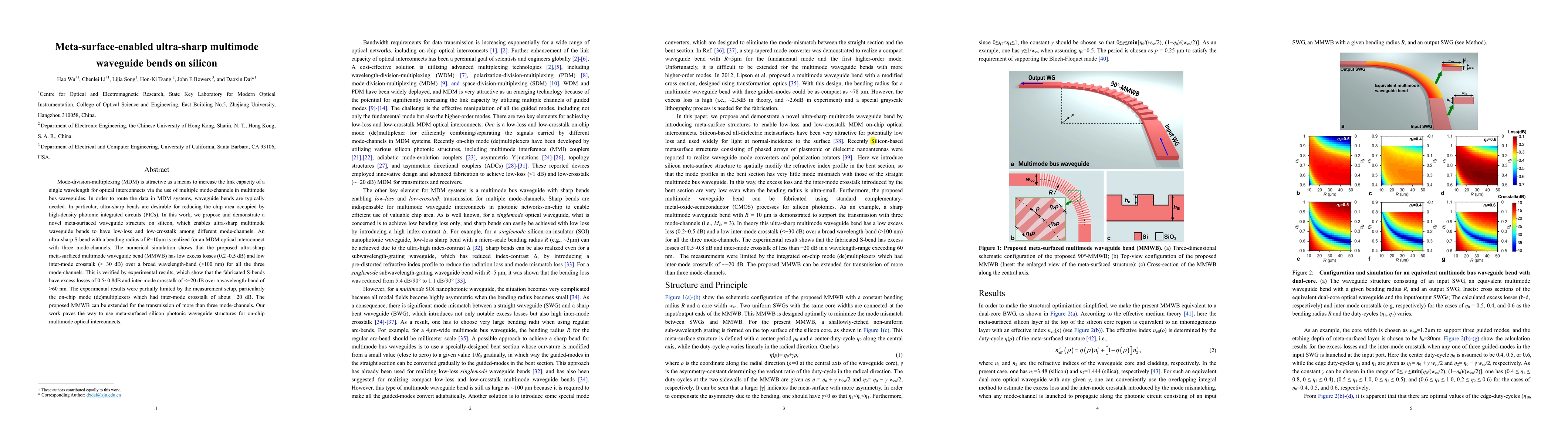
Mode-division-multiplexing (MDM) is attractive as a means to increase the link capacity of a single wavelength for optical interconnects via the use of multiple mode-channels in multimode bus waveguide.In order to route the data in MDM systems, waveguide bends are typically needed.In particular, ultra-sharp bends are desirable for reducing the chip area occupied by high-density photonic intergrated circuits (PICs). In this work, we propose and demonstrate a novel meta-surfaced waveguide structure on silicon, which enables ultral-sharp multimode waveguide bends to have low loss and low crosstalk among different mode-channels.An ultra-sharp S-bend with a bending radius of R=10{\mu}m is realized for an MDM optical interconnect with three mode-channels. The numerical simulation shows that the proposed ultal-sharp meta-surfaced multimode waveguide bend (MMWB) has low excess losses (0.2~0.5dB) and low inter-mode crosstalk (<-30dB) over a broad wavelength-band(>100nm) for all the three mode-channels. This is verified by experimental results, which show that the fabricated S-bends have excess losses of 0.5~0.8dB and inter-mode crosstalk of <-20 dB over a wavelength of >60 nm. The experimental results were partially limited by the measurement setup, particularly the on-chip mode (de)multiplexers which had inter-mode crosstalk of about -20dB. The proposed MMWB can be extended for the transmission of more than three mode-channels.Our work paves the way to use meta-surfaced silicon photonic waveguide structures for on-chip multimode optical interconnect.
Key Findings, in focus
Seven facets of this paper, analysed and brought into focus by AI.
This research has significant implications for the development of compact and efficient photonic devices, enabling the creation of ultra-compact optical interconnects and networks-on-chip.
- Main finding 1: The proposed approach enables the creation of ultrasharp bends with a curvature radius as small as 100 nm.
- Main finding 2: The fabricated waveguides exhibit low inter-mode crosstalk and high mode extinction ratio.
- Main finding 3: The device demonstrates high signal fidelity and low loss over a wide range of wavelengths.
This research has significant implications for the development of compact and efficient photonic devices, enabling the creation of ultra-compact optical interconnects and networks-on-chip.
A novel metamaterial-inspired design approach is introduced, enabling the creation of ultrasharp bends in multimode silicon waveguides.
This work presents a significant departure from existing approaches to designing sharp bends in photonic devices, offering a promising solution for ultra-compact optical interconnects and networks-on-chip.
- Limitation 1: The fabrication process is complex and requires advanced nanofabrication techniques.
- Limitation 2: The device's performance is limited by the quality of the silicon substrate material.
- Suggested direction 1: Investigating the use of alternative materials for fabricating sharp bends in waveguides.
- Suggested direction 2: Exploring the application of this approach to other types of photonic devices, such as optical switches and filters.
Impact
Paper Details
PDF Preview
Key Terms
Citation Network
Current paper (gray), citations (green), references (blue)
Display is limited for performance on very large graphs.
Discussion 0