ArxivLens

Publication

Published: Sep 26, 2025
Categories: physics.atom-ph

Metrics

Source: ArXiv

Quick Answers

What methodology did the authors use?

The research employs a wafer-level fabrication approach using laser-assisted etching (LAE) and thermal reflow of glass preforms bonded between silicon frames to create multi-axis alkali vapor cells with three orthogonal optical pathways. More in Methodology →

What are the key results?

Achieved magnetic sensitivities better than 200 fT/sqrt(Hz) along all three orthogonal axes. — Developed a fabrication process that enables embedded, optics-grade lateral windows through thermal reflow and surface smoothing techniques. More in Key Results →

Why is this work significant?

This work enables the creation of compact, high-performance atomic sensors compatible with mass production, which could revolutionize applications in magnetometry, gyroscopy, and other fields requiring precise magnetic field detection. More in Significance →

What are the main limitations?

Surface roughness remains an issue requiring thermal reflow, which may affect manufacturing efficiency. — Current buffer gas pressure is limited by bonding machine constraints, potentially limiting sensitivity improvements. More in Limitations →

Paper Preview

Abstract

Microfabricated alkali vapor cells enable the miniaturization of atomic sensors, but require collective wafer-level integration of complex features. In many applications, including magnetometers, gyroscopes, magneto-optical traps, and fluorescence imaging, multiple optical accesses are needed to enhance performance. Yet, achieving this without compromising manufacturability remains challenging. In this work, we present a wafer-level fabrication approach that enables three orthogonal optical pathways in microfabricated alkali vapor cells, using fully scalable and collective processes. Our method relies on the thermal reflow of glass preforms, shaped by laser-assisted etching (LAE) and bonded between silicon frames. The relatively low surface roughness produced by LAE allows effective reflow, which further smooths the surfaces without significantly compromising the optical planarity of the windows. This process results in multi-axis vapor cells featuring embedded, optics-grade lateral windows. We evaluate the device performance through both single-beam and dual-beam atomic magnetometry measurements. Magnetic sensitivities better than 200 fT/sqrt(Hz) are demonstrated along each of the three orthogonal axes, confirming the potential of the approach for tri-axis magnetic field sensing at sub-picotesla resolution. This fabrication strategy opens new perspectives for versatile, high-performance atomic sensors, fully compatible with wafer-level integration and mass production.
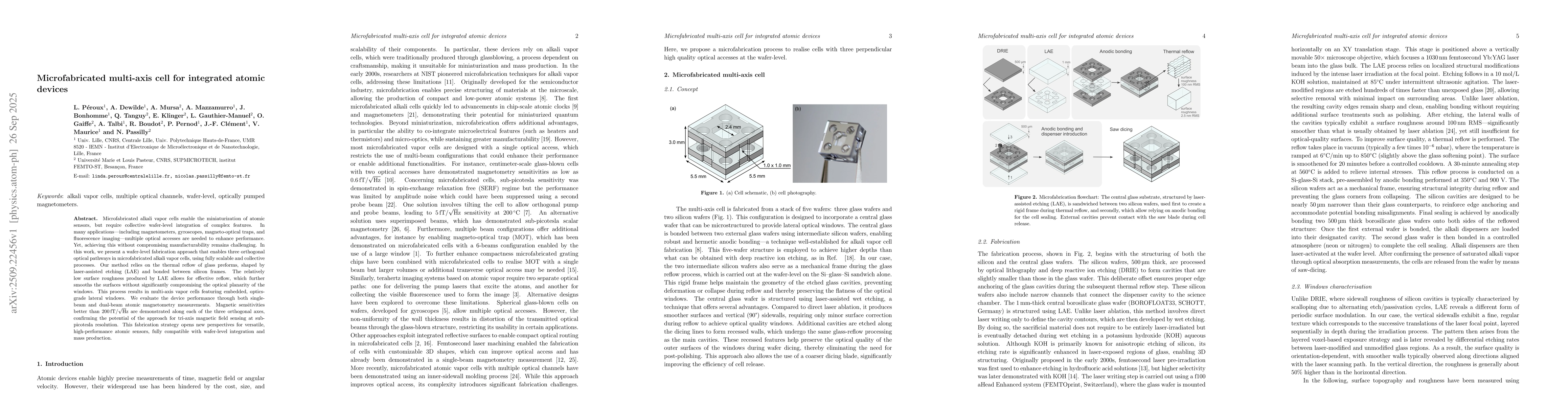
Key Findings, in focus

Seven facets of this paper, analysed and brought into focus by AI.

AI-generated · verify against source Generated Oct 01, 2025
In focus · one-line synthesis

This work enables the creation of compact, high-performance atomic sensors compatible with mass production, which could revolutionize applications in magnetometry, gyroscopy, and other fields requiring precise magnetic field detection.

01
MethodologyHow they did it

The research employs a wafer-level fabrication approach using laser-assisted etching (LAE) and thermal reflow of glass preforms bonded between silicon frames to create multi-axis alkali vapor cells with three orthogonal optical pathways.

02
ResultsWhat they found
  • Achieved magnetic sensitivities better than 200 fT/sqrt(Hz) along all three orthogonal axes.
  • Developed a fabrication process that enables embedded, optics-grade lateral windows through thermal reflow and surface smoothing techniques.
  • Demonstrated the feasibility of tri-axis magnetic field sensing at sub-picotesla resolution using the fabricated cells.
03
SignificanceWhy it matters

This work enables the creation of compact, high-performance atomic sensors compatible with mass production, which could revolutionize applications in magnetometry, gyroscopy, and other fields requiring precise magnetic field detection.

04
Technical ContributionsWhat's new technically

A scalable wafer-level fabrication technique combining LAE and thermal reflow to produce multi-axis vapor cells with high optical quality windows and integrated optical access.

05
NoveltyWhat sets it apart

The integration of laser-assisted etching with thermal reflow for surface smoothing, enabling high-quality optical windows without additional polishing, represents a novel approach to microfabrication of atomic devices.

06
LimitationsWhat to be cautious about
  • Surface roughness remains an issue requiring thermal reflow, which may affect manufacturing efficiency.
  • Current buffer gas pressure is limited by bonding machine constraints, potentially limiting sensitivity improvements.
07
Future WorkWhere it goes next
  • Exploring methods to increase buffer gas pressure for enhanced sensitivity.
  • Investigating ways to improve lateral window dimensions and optical quality for better performance.
  • Developing external filling methods to eliminate internal dispensers and allow higher gas pressures.

Paper Details

Paper ID: 2509.22456
Comments: 13 pages, 5 figures
Categories:
physics.atom-ph

How to Cite This Paper

Reference manager: RIS EndNote


Discussion 0

This website uses cookies to ensure you get the best experience. Learn more