Mid-infrared GeSn Electro-Absorption Optical Modulators on Silicon
Publication
Metrics
AI Quick Summary
This paper presents a GeSn electro-absorption modulator for mid-infrared optical communication, achieving optimal modulation in the range of 2067-2208 nm. The device is monolithically integrated on silicon, enabling compatibility with existing CMOS technology for scalable manufacturing.
Paper Preview
Abstract
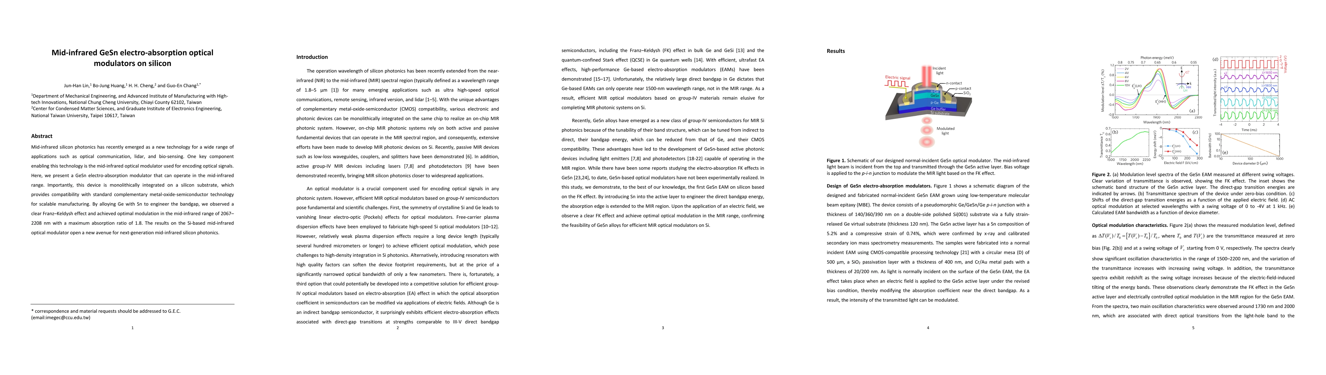
Mid-infrared silicon photonics has recently emerged as a new technology for a wide range of applications such as optical communication, lidar, and bio-sensing. One key component enabling this technology is the mid-infrared optical modulator used for encoding optical signals. Here, we present a GeSn electro-absorption modulator that can operate in the mid-infrared range. Importantly, this device is monolithically integrated on a silicon substrate, which provides compatibility with standard complementary metal-oxide-semiconductor technology for scalable manufacturing. By alloying Ge with Sn to engineer the bandgap, we observed a clear Franz-Keldysh effect and achieved optimal modulation in the mid-infrared range of 2067-2208 nm with a maximum absorption ratio of 1.8. The results on the Si-based mid-infrared optical modulator open a new avenue for next-generation mid-infrared silicon photonics.
AI Key Findings
Get AI-generated insights about this paper's methodology, results, significance, and more — seven facets brought into focus.
Impact
Paper Details
PDF Preview
Key Terms
Citation Network
Current paper (gray), citations (green), references (blue)
Display is limited for performance on very large graphs.
Discussion 0