01
MethodologyHow they did it
A combined simulation and experimental approach was used to analyze GaN HEMTs.
A combined simulation and experimental approach was used to analyze GaN HEMTs. More in Methodology →
The device demonstrated an ON current of 1.9 mA and an OFF current of 0.01 mA. — A subthreshold swing of 80 mV/decade and a DIBL of 5 mV/V were observed. More in Key Results →
This research is important for understanding GaN HEMT behavior and optimizing device performance for high-power and RF applications. More in Significance →
The analysis focused on a single device, which may not be representative of all GaN HEMTs. — The study did not investigate the effects of temperature or other environmental factors on device performance. More in Limitations →
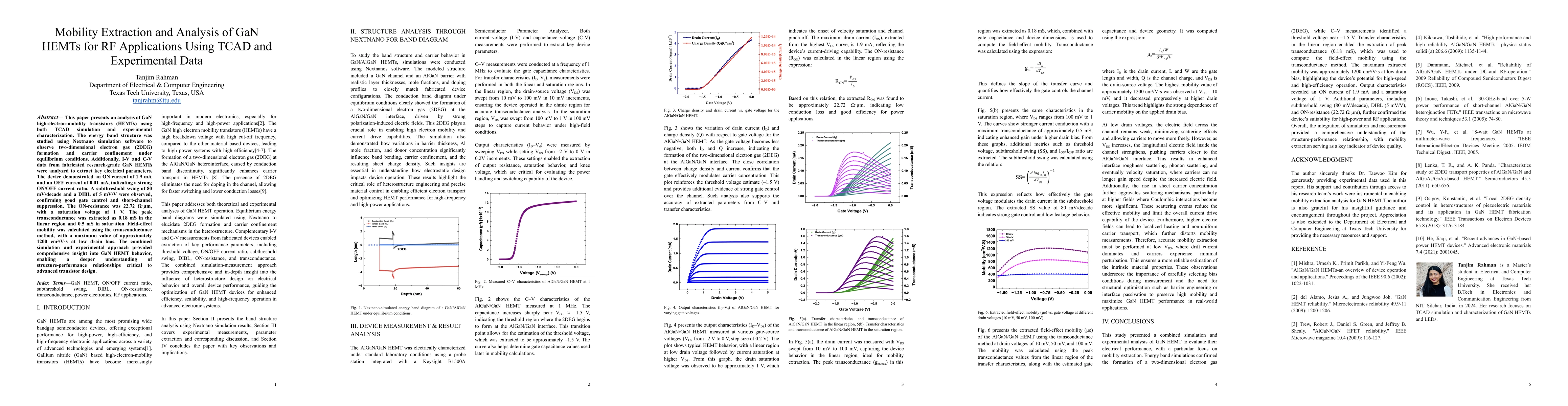
This paper presents an analysis of GaN high-electron-mobility transistors (HEMTs) using both TCAD simulation and experimental characterization. The energy band structure was studied using Nextnano simulation software to observe two-dimensional electron gas (2DEG) formation and carrier confinement under equilibrium conditions. Additionally, I-V and C-V data from fabricated research-grade GaN HEMTs were analyzed to extract key electrical parameters. The device demonstrated an ON current of 1.9 mA and an OFF current of 0.01 mA, indicating a strong ON/OFF current ratio. A subthreshold swing of 80 mV/decade and a DIBL of 5 mV/V were observed, confirming good gate control and short-channel suppression. The ON-resistance was 22.72 ohm per micron, with a saturation voltage of 1 V . The peak transconductance was extracted as 0.18 mS in the linear region and 0.5 mS in saturation. Field-effect mobility was calculated using the transconductance method, with a maximum value of approximately 1200 cm2/V.s at low drain bias. The combined simulation and experimental approach provided comprehensive insight into GaN HEMT behavior, enabling a deeper understanding of structure-performance relationships critical to advanced transistor design.
Seven facets of this paper, analysed and brought into focus by AI.
This research is important for understanding GaN HEMT behavior and optimizing device performance for high-power and RF applications.
A combined simulation and experimental approach was used to analyze GaN HEMTs.
This research is important for understanding GaN HEMT behavior and optimizing device performance for high-power and RF applications.
The study presented a comprehensive understanding of GaN HEMT structure-performance relationships using TCAD simulation and experimental characterization.
This work highlights the importance of combining simulation and measurement techniques for optimizing GaN HEMT performance, particularly in high-power and RF applications.
No references found for this paper.
Discussion 0