ArxivLens

Publication

Published: May 01, 2025
Categories: physics.optics, quant-ph

Metrics

Source: ArXiv

AI Quick Summary

Researchers successfully created scalable nanobeam cavities on silicon for C-band quantum emitters, achieving up to 500-fold Purcell enhancement and demonstrating a path to manufacturable single-photon sources.

Quick Answers

What is "Monolithically Integrated C-Band Quantum Emitters on Foundry Silicon Photonics" about?

Researchers successfully created scalable nanobeam cavities on silicon for C-band quantum emitters, achieving up to 500-fold Purcell enhancement and demonstrating a path to manufacturable single-photon sources.

What methodology did the authors use?

The research demonstrates high-quality factor, small mode volume nanobeam cavities fabricated on a scalable silicon photonic foundry platform, interfaced with single erbium ions through backend deposition of TiO2 thin films lightly doped with erbium. More in Methodology →

What are the key results?

High quality factor, small mode volume nanobeam cavities fabricated on a scalable silicon photonic foundry platform. — Single erbium ions interfaced with the cavities, showing Purcell enhancement up to about 500. More in Key Results →

Why is this work significant?

This work is significant as it presents a scalable approach for developing single-photon emitters with spin-photon interfaces in the telecom C-band, which is crucial for future quantum networking systems such as quantum interconnects and quantum repeaters. More in Significance →

What are the main limitations?

The study did not utilize the highest quality factor cavities available on the chip. — Further improvements could be achieved by optimizing material deposition and post-growth treatment for narrower emitter linewidths. More in Limitations →

Paper Preview

Abstract

Solid-state spin-based quantum systems have emerged as popular platforms for 
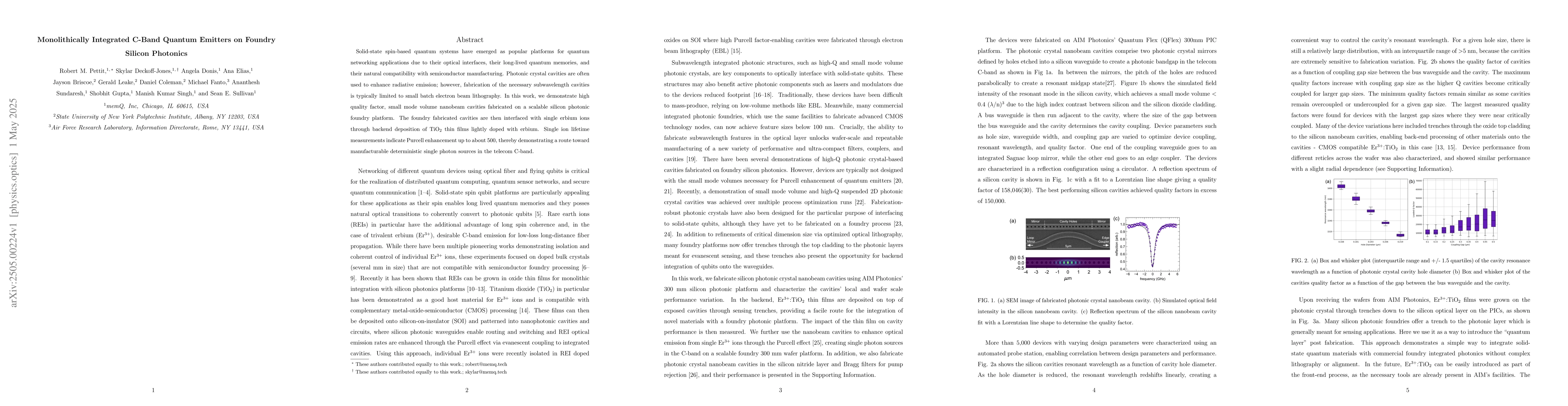
quantum networking applications due to their optical interfaces, their long-lived quantum memories, and their natural compatibility with semiconductor manufacturing. Photonic crystal cavities are often used to enhance radiative emission; however, fabrication of the necessary subwavelength cavities is typically limited to small batch electron beam lithography. In this work, we demonstrate high quality factor, small mode volume nanobeam cavities fabricated on a scalable silicon photonic foundry platform. The foundry fabricated cavities are then interfaced with single erbium ions through backend deposition of TiO2 thin films lightly doped with erbium. Single ion lifetime measurements indicate Purcell enhancement up to about 500, thereby demonstrating a route toward manufacturable deterministic single photon sources in the telecom C-band.

Key Findings, in focus

Seven facets of this paper, analysed and brought into focus by AI.

AI-generated · verify against source Generated May 28, 2025
In focus · one-line synthesis

This work is significant as it presents a scalable approach for developing single-photon emitters with spin-photon interfaces in the telecom C-band, which is crucial for future quantum networking systems such as quantum interconnects and quantum repeaters.

01
MethodologyHow they did it

The research demonstrates high-quality factor, small mode volume nanobeam cavities fabricated on a scalable silicon photonic foundry platform, interfaced with single erbium ions through backend deposition of TiO2 thin films lightly doped with erbium.

02
ResultsWhat they found
  • High quality factor, small mode volume nanobeam cavities fabricated on a scalable silicon photonic foundry platform.
  • Single erbium ions interfaced with the cavities, showing Purcell enhancement up to about 500.
  • Demonstrated a route toward manufacturable deterministic single photon sources in the telecom C-band.
03
SignificanceWhy it matters

This work is significant as it presents a scalable approach for developing single-photon emitters with spin-photon interfaces in the telecom C-band, which is crucial for future quantum networking systems such as quantum interconnects and quantum repeaters.

04
Technical ContributionsWhat's new technically

The paper presents a method for monolithic integration of C-band quantum emitters on foundry silicon photonics, utilizing backend deposition of Er3+:TiO2 thin films for interfacing with single erbium ions in nanobeam photonic crystal cavities.

05
NoveltyWhat sets it apart

The novelty of this work lies in the scalable fabrication of high-quality photonic crystal cavities on a silicon photonic foundry platform and the successful integration of Er3+:TiO2 thin films for single-photon emission in the telecom C-band.

06
LimitationsWhat to be cautious about
  • The study did not utilize the highest quality factor cavities available on the chip.
  • Further improvements could be achieved by optimizing material deposition and post-growth treatment for narrower emitter linewidths.
07
Future WorkWhere it goes next
  • Exploration of higher quality factor cavities for shorter optical lifetimes and increased radiative linewidth limits.
  • Tailoring the thickness of thin film buffering layers and implementing surface passivation techniques to reduce ion proximity to interfaces.

Impact

35
References

Paper Details

Paper ID: 2505.00224
Categories:
physics.optics quant-ph

How to Cite This Paper

Reference manager: RIS EndNote

Citation Network

Current paper (gray), citations (green), references (blue)

Display is limited for performance on very large graphs.

Current Paper
Citations
References
Click to view


Discussion 0

This website uses cookies to ensure you get the best experience. Learn more