Multispectral UV Imaging on Capacitive CMOS Arrays Enabled by Solution-Processed Metal-Oxide Nanoparticles
Publication
Metrics
Paper Preview
Abstract
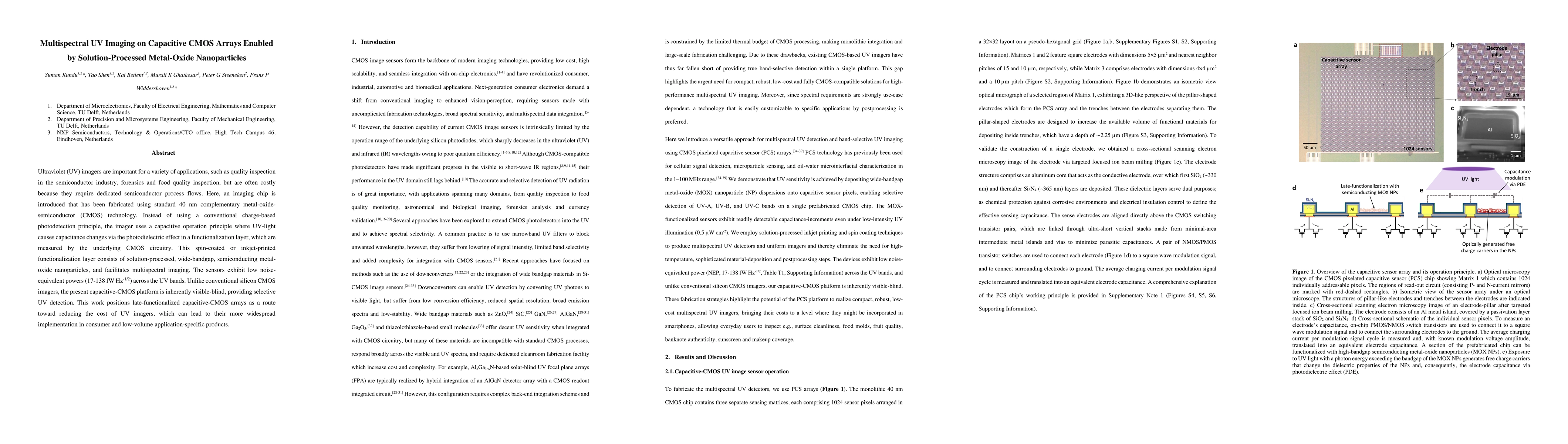
Ultraviolet (UV) imagers are important for a variety of applications, such as quality inspection in the semiconductor industry, forensics and food quality inspection, but are often costly because they require dedicated semiconductor process flows. Here, an imaging chip is introduced that has been fabricated using standard 40 nm complementary metal-oxidesemiconductor (CMOS) technology. Instead of using a conventional charge-based photodetection principle, the imager uses a capacitive operation principle where UV-light causes capacitance changes via the photodielectric effect in a functionalization layer, which are measured by the underlying CMOS circuitry. This spin-coated or inkjet-printed functionalization layer consists of solution-processed, wide-bandgap, semiconducting metaloxide nanoparticles, and facilitates multispectral imaging. The sensors exhibit low noiseequivalent powers (17-138 fW Hz^-1/2) across the UV bands. Unlike conventional silicon CMOS imagers, the present capacitive-CMOS platform is inherently visible-blind, providing selective UV detection. This work positions late-functionalized capacitive-CMOS arrays as a route toward reducing the cost of UV imagers, which can lead to their more widespread implementation in consumer and low-volume application-specific products.
AI Key Findings
Get AI-generated insights about this paper's methodology, results, significance, and more — seven facets brought into focus.
Discussion 0