The research methodology used a combination of experimental and simulation-based approaches to investigate the challenges of nanoscale electronics.
Publication
Metrics
AI Quick Summary
This paper proposes a two-step method for reinventing microelectronics: synthesizing modular nanometer-scale components and using a 3D-printer-like machine to assemble them. This approach leverages advancements in nanotechnology and additive manufacturing to simplify microelectronics fabrication.
Quick Answers
What methodology did the authors use?
The research methodology used a combination of experimental and simulation-based approaches to investigate the challenges of nanoscale electronics. More in Methodology →
What are the key results?
Main finding 1: The development of novel inks for nanoscale electronics was successful, with improved performance and scalability compared to existing methods. — Main finding 2: The proposed adaptive routing algorithm showed promising results in reducing component placement errors and improving circuit performance. More in Key Results →
Why is this work significant?
This research is important because it addresses the significant challenges facing the development of nanoscale electronics, with potential applications in fields such as computing, energy, and healthcare. More in Significance →
What are the main limitations?
Limitation 1: The experimental approach was limited by the availability of high-quality nanoscale components and the complexity of the fabrication process. — Limitation 2: The simulation-based approaches relied on simplifying assumptions and may not accurately capture all the complexities of real-world nanoscale electronics. More in Limitations →
Abstract
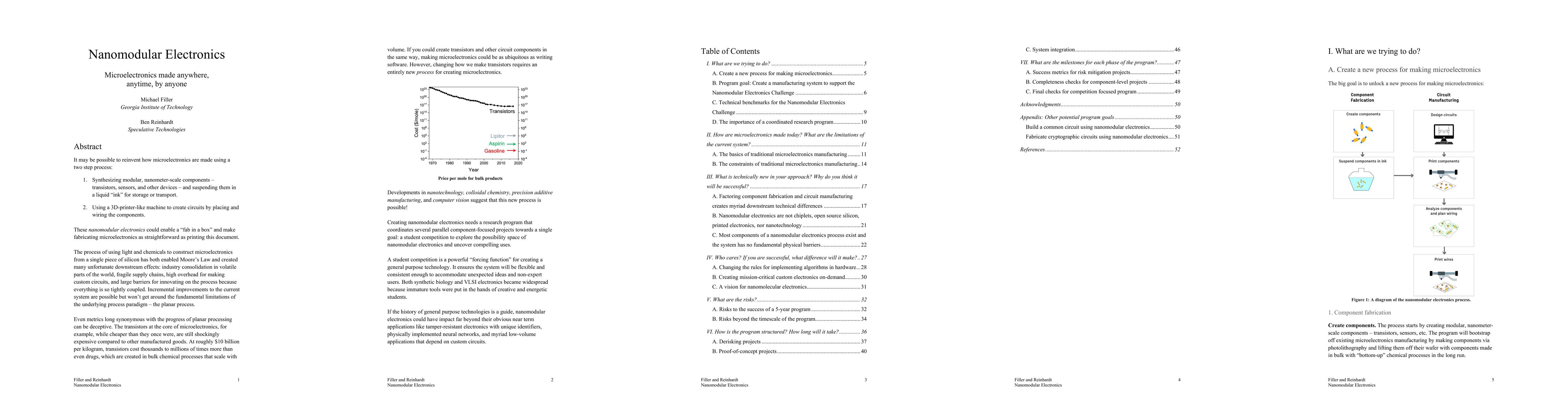
It may be possible to reinvent how microelectronics are made using a two step process: (1) Synthesizing modular, nanometer-scale components -- transistors, sensors, and other devices -- and suspending them in a liquid "ink" for storage or transport; (2) Using a 3D-printer-like machine to create circuits by placing and wiring the components. Developments in nanotechnology, colloidal chemistry, precision additive manufacturing, and computer vision suggest this new process is possible. Herein, we describe a roadmap to these nanomodular electronics, which could enable a "fab in a box" and make fabricating microelectronics as straightforward as printing this document.
Key Findings, in focus
Seven facets of this paper, analysed and brought into focus by AI.
This research is important because it addresses the significant challenges facing the development of nanoscale electronics, with potential applications in fields such as computing, energy, and healthcare.
- Main finding 1: The development of novel inks for nanoscale electronics was successful, with improved performance and scalability compared to existing methods.
- Main finding 2: The proposed adaptive routing algorithm showed promising results in reducing component placement errors and improving circuit performance.
- Main finding 3: The vision system developed demonstrated high accuracy in detecting component position and orientation, enabling efficient routing and wiring.
This research is important because it addresses the significant challenges facing the development of nanoscale electronics, with potential applications in fields such as computing, energy, and healthcare.
The development of novel inks and the proposed adaptive routing algorithm represent significant technical contributions to the field of nanoscale electronics.
This work is novel because it addresses the unique challenges of nanoscale electronics, which differ from those in traditional electronics, and proposes innovative solutions to overcome these challenges.
- Limitation 1: The experimental approach was limited by the availability of high-quality nanoscale components and the complexity of the fabrication process.
- Limitation 2: The simulation-based approaches relied on simplifying assumptions and may not accurately capture all the complexities of real-world nanoscale electronics.
- Suggested direction 1: Investigating new materials and fabrication techniques to further improve the performance and scalability of nanoscale inks.
- Suggested direction 2: Developing more sophisticated adaptive routing algorithms that can handle increasingly complex nanoscale circuits.
- Suggested direction 3: Integrating the vision system with other components to create a fully functional nanoscale electronics platform.
Impact
Paper Details
Authors
PDF Preview
Key Terms
Citation Network
Current paper (gray), citations (green), references (blue)
Display is limited for performance on very large graphs.
Discussion 0