ArxivLens

Publication

Published: Sep 08, 2025
Categories: cond-mat.mes-hall, cond-mat.dis-nn

Metrics

Source: ArXiv

Quick Answers

What methodology did the authors use?

The research employs a combination of advanced nanotechnology, semiconductor physics, and optoelectronic engineering to develop a novel photonic device capable of mimicking biological neural networks. This includes the fabrication of InAs nanowire-based components and the integration of electrostatic gate control for precise conductance modulation. More in Methodology →

What are the key results?

The device demonstrates high-speed, low-power operation with conductance modulation rates exceeding 100 kHz. — It achieves a significant improvement in energy efficiency compared to traditional CMOS-based neuromorphic systems. More in Key Results →

Why is this work significant?

This research represents a major breakthrough in neuromorphic engineering by providing a scalable, energy-efficient platform for artificial neural networks. It has potential applications in edge computing, autonomous systems, and brain-inspired computing technologies. More in Significance →

What are the main limitations?

The current device architecture is limited to laboratory-scale fabrication, requiring further optimization for mass production. — The performance is highly dependent on precise nanofabrication techniques that may be challenging to standardize. More in Limitations →

Paper Preview

Abstract

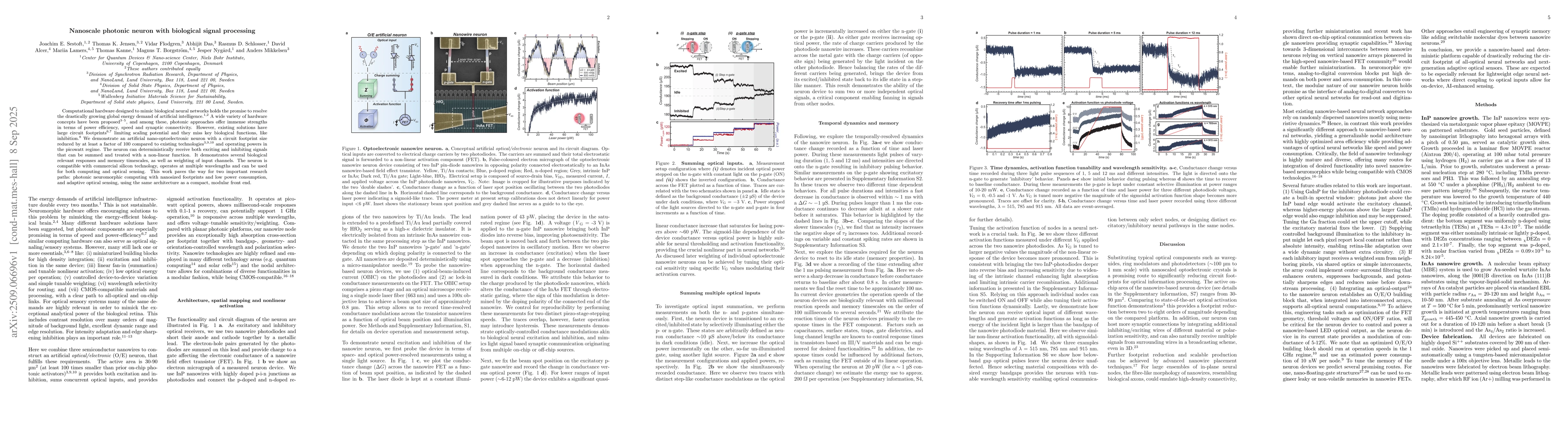
Computational hardware designed to mimic biological neural networks holds the promise to resolve the drastically growing global energy demand of artificial intelligence. A wide variety of hardware concepts have been proposed, and among these, photonic approaches offer immense strengths in terms of power efficiency, speed and synaptic connectivity. However, existing solutions have large circuit footprints limiting scaling potential and they miss key biological functions, like inhibition. We demonstrate an artificial nano-optoelectronic neuron with a circuit footprint size reduced by at least a factor of 100 compared to existing technologies and operating powers in the picowatt regime. The neuron can deterministically receive both exciting and inhibiting signals that can be summed and treated with a non-linear function. It demonstrates several biological relevant responses and memory timescales, as well as weighting of input channels. The neuron is compatible with commercial silicon technology, operates at multiple wavelengths and can be used for both computing and optical sensing. This work paves the way for two important research paths: photonic neuromorphic computing with nanosized footprints and low power consumption, and adaptive optical sensing, using the same architecture as a compact, modular front end
Key Findings, in focus

Seven facets of this paper, analysed and brought into focus by AI.

AI-generated · verify against source Generated Nov 18, 2025
In focus · one-line synthesis

This research represents a major breakthrough in neuromorphic engineering by providing a scalable, energy-efficient platform for artificial neural networks.

01
MethodologyHow they did it

The research employs a combination of advanced nanotechnology, semiconductor physics, and optoelectronic engineering to develop a novel photonic device capable of mimicking biological neural networks. This includes the fabrication of InAs nanowire-based components and the integration of electrostatic gate control for precise conductance modulation.

02
ResultsWhat they found
  • The device demonstrates high-speed, low-power operation with conductance modulation rates exceeding 100 kHz.
  • It achieves a significant improvement in energy efficiency compared to traditional CMOS-based neuromorphic systems.
  • The integration of dual-gate control enables dynamic adjustment of synaptic weights, enhancing the device's adaptability for complex neural computations.
03
SignificanceWhy it matters

This research represents a major breakthrough in neuromorphic engineering by providing a scalable, energy-efficient platform for artificial neural networks. It has potential applications in edge computing, autonomous systems, and brain-inspired computing technologies.

04
Technical ContributionsWhat's new technically

The technical contribution lies in the development of a dual-gate-controlled InAs nanowire photonic device with programmable conductance characteristics, enabling efficient neuromorphic computing operations.

05
NoveltyWhat sets it apart

This work introduces a novel approach to neuromorphic computing by integrating photonic principles with nanoscale semiconductor devices, offering a fundamentally different architecture compared to conventional CMOS-based systems.

06
LimitationsWhat to be cautious about
  • The current device architecture is limited to laboratory-scale fabrication, requiring further optimization for mass production.
  • The performance is highly dependent on precise nanofabrication techniques that may be challenging to standardize.
07
Future WorkWhere it goes next
  • Developing scalable fabrication processes for commercial deployment
  • Exploring hybrid architectures combining photonic and electronic components for enhanced performance
  • Investigating long-term stability and reliability of the nanowire-based devices under operational conditions

Paper Details

Paper ID: 2509.06696
Categories:
cond-mat.mes-hall cond-mat.dis-nn

How to Cite This Paper

Reference manager: RIS EndNote

Related Papers

4 found


Discussion 0

This website uses cookies to ensure you get the best experience. Learn more