Novel Electrostatically Doped Planar Field-Effect Transistor for High Temperature Applications
Publication
Metrics
AI Quick Summary
This paper introduces a novel electrostatically doped planar field-effect transistor (FET) based on Si-nanowire technology, featuring dual-gated operation for enhanced temperature robustness. The device combines Si-nanowire, Schottky barrier contacts, and a silicon-on-insulator platform for improved high-temperature performance.
Paper Preview
Abstract
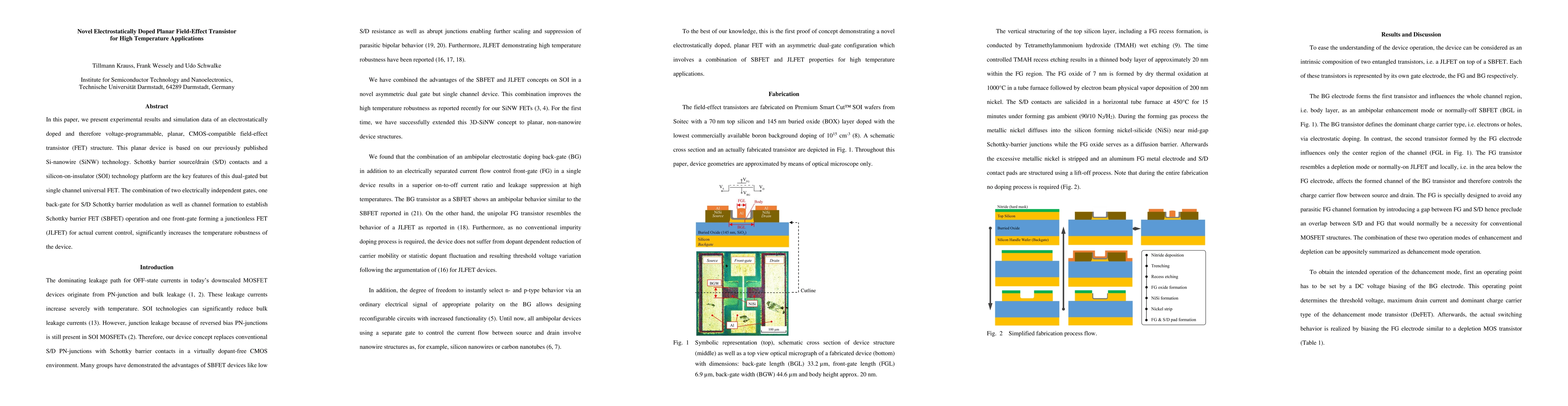
In this paper, we present experimental results and simulation data of an electrostatically doped and therefore voltage-programmable, planar, CMOS-compatible field-effect transistor (FET) structure. This planar device is based on our previously published Si-nanowire (SiNW) technology. Schottky barrier source/drain (S/D) contacts and a silicon-on-insulator (SOI) technology platform are the key features of this dual-gated but single channel universal FET. The combination of two electrically independent gates, one back-gate for S/D Schottky barrier modulation as well as channel formation to establish Schottky barrier FET (SBFET) operation and one front-gate forming a junctionless FET (JLFET) for actual current control, significantly increases the temperature robustness of the device.
AI Key Findings
Get AI-generated insights about this paper's methodology, results, significance, and more — seven facets brought into focus.
Impact
Paper Details
PDF Preview
Key Terms
Citation Network
Current paper (gray), citations (green), references (blue)
Display is limited for performance on very large graphs.
Discussion 0