Plasmonic nanogap enhanced phase change devices with dual electrical-optical functionality
Publication
Metrics
AI Quick Summary
This paper introduces a novel plasmonic nanogap-enhanced phase change device that integrates electrical and optical functionalities, enabling seamless on-chip computing and communication. The device can be electrically or optically switched between binary or multilevel states, merging computing and communications technologies.
Paper Preview
Abstract
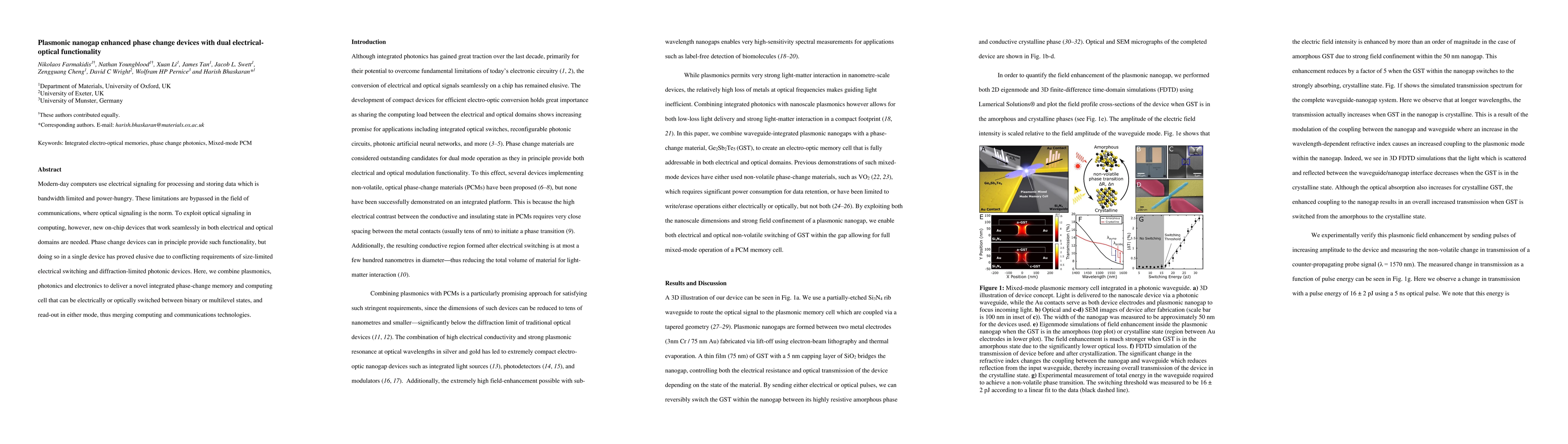
Modern-day computers use electrical signaling for processing and storing data which is bandwidth limited and power-hungry. These limitations are bypassed in the field of communications, where optical signaling is the norm. To exploit optical signaling in computing, however, new on-chip devices that work seamlessly in both electrical and optical domains are needed. Phase change devices can in principle provide such functionality, but doing so in a single device has proved elusive due to conflicting requirements of size-limited electrical switching and diffraction-limited photonic devices. Here, we combine plasmonics, photonics and electronics to deliver a novel integrated phase-change memory and computing cell that can be electrically or optically switched between binary or multilevel states, and read-out in either mode, thus merging computing and communications technologies.
AI Key Findings
Get AI-generated insights about this paper's methodology, results, significance, and more — seven facets brought into focus.
Impact
Paper Details
PDF Preview
Key Terms
Citation Network
Current paper (gray), citations (green), references (blue)
Display is limited for performance on very large graphs.
Discussion 0