Publication
Metrics
AI Quick Summary
This paper presents a novel method for growing an InP-based distributed feedback laser array directly on silicon using selective area growth, achieving high performance and uniformity at room temperature. This breakthrough enables scalable integration with photonic circuits and III-V FINFET logic, paving the way for cost-effective co-integration.
Paper Preview
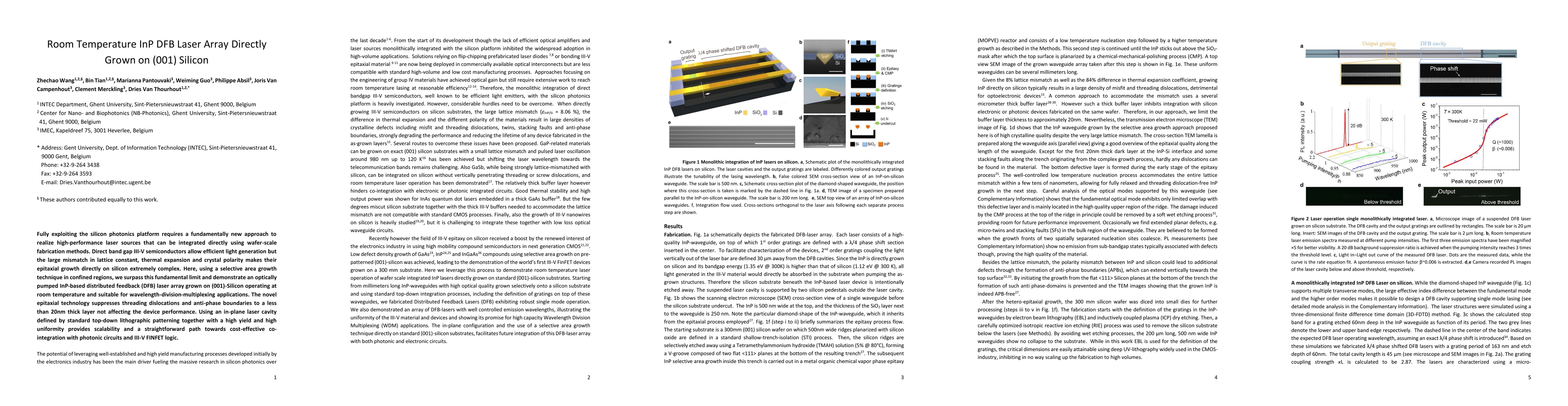
Abstract
Fully exploiting the silicon photonics platform requires a fundamentally new approach to realize high-performance laser sources that can be integrated directly using wafer-scale fabrication methods. Direct band gap III-V semiconductors allow efficient light generation but the large mismatch in lattice constant, thermal expansion and crystal polarity makes their epitaxial growth directly on silicon extremely complex. Here, using a selective area growth technique in confined regions, we surpass this fundamental limit and demonstrate an optically pumped InP-based distributed feedback (DFB) laser array grown on (001)-Silicon operating at room temperature and suitable for wavelength-division-multiplexing applications. The novel epitaxial technology suppresses threading dislocations and anti-phase boundaries to a less than 20nm thick layer not affecting the device performance. Using an in-plane laser cavity defined by standard top-down lithographic patterning together with a high yield and high uniformity provides scalability and a straightforward path towards cost-effective co-integration with photonic circuits and III-V FINFET logic.
AI Key Findings
Get AI-generated insights about this paper's methodology, results, significance, and more — seven facets brought into focus.
Impact
Paper Details
PDF Preview
Key Terms
Citation Network
Current paper (gray), citations (green), references (blue)
Display is limited for performance on very large graphs.
Discussion 0