ArxivLens

Publication

Published: Jul 11, 2026
Categories: cs.CV

Metrics

Source: ArXiv

Quick Answers

What methodology did the authors use?

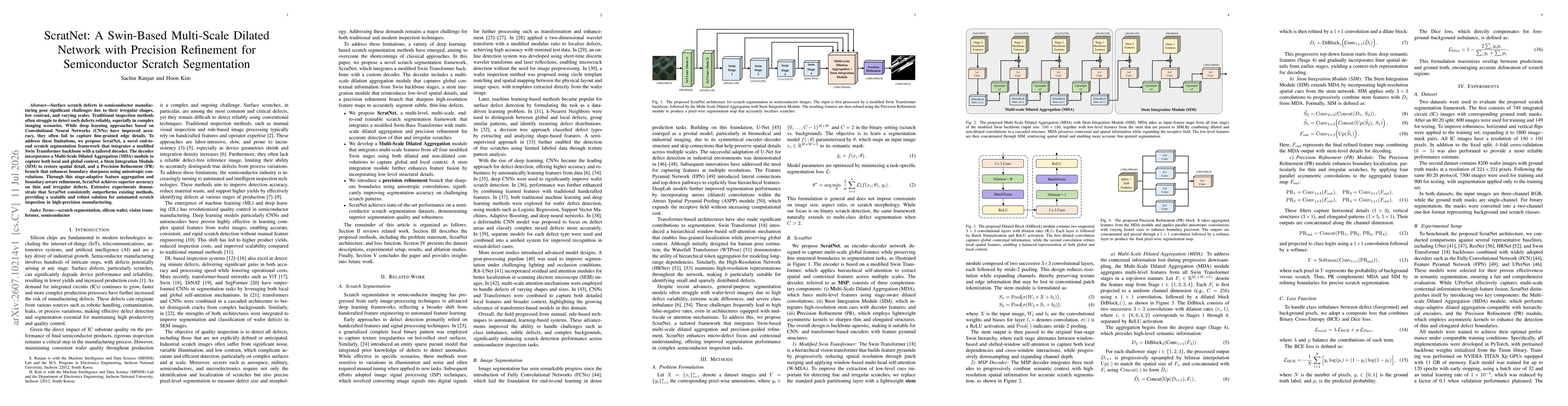
ScratNet introduces a modified Swin Transformer backbone integrated with a custom decoder. The decoder combines a Multi-Scale Dilated Aggregation (MDA) module to fuse multi-scale features from all Swin stages, a Stem Integration Module (SIM) to reintroduce low-level spatial details, and a Precision Refinement (PR) branch that uses anisotropic convolutions to sharpen object boundaries. The network is trained end-to-end for pixel-level... More in Methodology →

What are the key results?

ScratNet achieves state-of-the-art segmentation performance on semiconductor scratch datasets, delivering higher boundary precision and better handling of thin defects compared with existing methods. — The MDA module effectively fuses global and local context from multiple Swin stages, improving segmentation of irregular scratch shapes. More in Key Results →

Why is this work significant?

The framework provides a scalable, robust end-to-end solution for automated wafer scratch inspection, addressing the challenge of thin, low-contrast, and irregular defects and potentially improving yield and quality control in high-precision semiconductor manufacturing. More in Significance →

What are the main limitations?

Evaluation is primarily on scratch segmentation benchmarks; real-world deployment may require further validation across diverse imaging modalities and defect morphologies. — Computational complexity increases due to multi-scale fusion and anisotropic refinements, which may impact inference speed on resource-constrained systems. More in Limitations →

Paper Preview

Abstract

Surface scratch defects in semiconductor manufacturing pose significant challenges due to their irregular shapes, low contrast, and varying scales. Traditional inspection methods often struggle to detect such defects reliably, especially in complex imaging scenarios. While deep learning approaches based on Convolutional Neural Networks (CNNs) have improved accuracy, they often fail to capture fine-grained edge details. To address these limitations, we propose ScratNet, a novel end-to-end scratch segmentation framework that integrates a modified Swin Transformer backbone with a tailored decoder. The decoder incorporates a Multi-Scale Dilated Aggregation (MDA) module to capture both local and global context, a Stem Integration Module (SIM) to restore spatial detail, and a Precision Refinement (PR) branch that enhances boundary sharpness using anisotropic convolutions. Through this stage-adaptive feature aggregation and boundary-aware refinement, ScratNet achieves superior accuracy on thin and irregular defects. Extensive experiments demonstrate that ScratNet consistently outperforms existing methods, providing a scalable and robust solution for automated scratch inspection in high-precision manufacturing.

Key Findings, in focus

Seven facets of this paper, analysed and brought into focus by AI.

AI-generated · verify against source Generated Jul 14, 2026
In focus · one-line synthesis

The framework provides a scalable, robust end-to-end solution for automated wafer scratch inspection, addressing the challenge of thin, low-contrast, and irregular defects and potentially improving yield and quality control in high-precision semiconductor manufacturing.

01
MethodologyHow they did it

ScratNet introduces a modified Swin Transformer backbone integrated with a custom decoder. The decoder combines a Multi-Scale Dilated Aggregation (MDA) module to fuse multi-scale features from all Swin stages, a Stem Integration Module (SIM) to reintroduce low-level spatial details, and a Precision Refinement (PR) branch that uses anisotropic convolutions to sharpen object boundaries. The network is trained end-to-end for pixel-level scratch segmentation, employing stage-adaptive feature aggregation to capture thin and irregular defects under challenging imaging conditions.

02
ResultsWhat they found
  • ScratNet achieves state-of-the-art segmentation performance on semiconductor scratch datasets, delivering higher boundary precision and better handling of thin defects compared with existing methods.
  • The MDA module effectively fuses global and local context from multiple Swin stages, improving segmentation of irregular scratch shapes.
  • The SIM and PR branch significantly enhance boundary sharpness and spatial detail, leading to more accurate pixel-level delineation of scratches.
03
SignificanceWhy it matters

The framework provides a scalable, robust end-to-end solution for automated wafer scratch inspection, addressing the challenge of thin, low-contrast, and irregular defects and potentially improving yield and quality control in high-precision semiconductor manufacturing.

04
Technical ContributionsWhat's new technically

A novel ScratNet architecture that combines a modified Swin Transformer backbone with a Multi-Scale Dilated Aggregation module, a Stem Integration Module for details restoration, and a Precision Refinement branch with anisotropic convolutions to sharpen scratch boundaries, enabling precise pixel-wise segmentation.

05
NoveltyWhat sets it apart

Introduces a stage-aware, multi-scale dilation fusion strategy within a Swin-Transformer framework specifically tailored for semiconductor scratch segmentation, along with a boundary-focused refinement branch to address thin and irregular defect shapes.

06
LimitationsWhat to be cautious about
  • Evaluation is primarily on scratch segmentation benchmarks; real-world deployment may require further validation across diverse imaging modalities and defect morphologies.
  • Computational complexity increases due to multi-scale fusion and anisotropic refinements, which may impact inference speed on resource-constrained systems.
07
Future WorkWhere it goes next
  • Explore lightweight variants of ScratNet for real-time inspection in production lines.
  • Extend the approach to related surface defects beyond scratches, such as stains or pinholes, to assess generalizability.
  • Integrate self-supervised or semi-supervised learning to reduce annotated data requirements for new wafer processes.

Paper Details

Paper ID: 2607.10214
Categories:
cs.CV

How to Cite This Paper

Reference manager: RIS EndNote


Discussion 0

This website uses cookies to ensure you get the best experience. Learn more