Publication
Metrics
AI Quick Summary
This paper reports the creation of a 2D p-n junction diode using electrostatically doped tungsten diselenide monolayer, demonstrating applications in photovoltaic solar cells, photodiodes, and light-emitting diodes with conversion and electroluminescence efficiencies of approximately 0.5% and 0.1%, respectively. The findings suggest significant potential for 2D atomic crystals in future optoelectronic technologies.
Paper Preview
Abstract
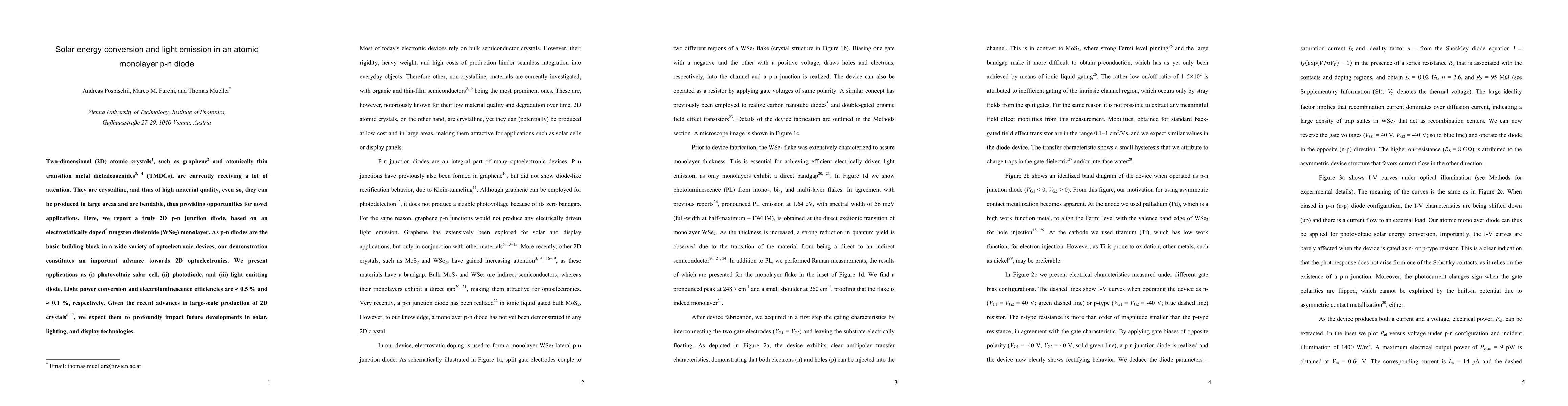
Two-dimensional (2D) atomic crystals, such as graphene and atomically thin transition metal dichalcogenides (TMDCs), are currently receiving a lot of attention. They are crystalline, and thus of high material quality, even so, they can be produced in large areas and are bendable, thus providing opportunities for novel applications. Here, we report a truly 2D p-n junction diode, based on an electrostatically doped tungsten diselenide (WSe2) monolayer. As p-n diodes are the basic building block in a wide variety of optoelectronic devices, our demonstration constitutes an important advance towards 2D optoelectronics. We present applications as (i) photovoltaic solar cell, (ii) photodiode, and (iii) light emitting diode. Light power conversion and electroluminescence efficiencies are ca. 0.5 % and 0.1 %, respectively. Given the recent advances in large-scale production of 2D crystals, we expect them to profoundly impact future developments in solar, lighting, and display technologies.
AI Key Findings
Get AI-generated insights about this paper's methodology, results, significance, and more — seven facets brought into focus.
Impact
Paper Details
PDF Preview
Key Terms
Citation Network
Current paper (gray), citations (green), references (blue)
Display is limited for performance on very large graphs.
Discussion 0