A UV‑tape‑assisted laser patterning (UT‑Laser) process was used to vector‑cut thin metal foils or films on UV tape, selectively UV‑expose the tape to control adhesive strength, peel away excess material, transfer the fine wiring onto a glass cloth textile substrate, and then solder rigid electronic components onto the patterned wiring using standard PCB processes
Solderable Microcontroller-Integrated E-Textiles using UV-Tape-Assisted Laser Patterning Technique
Publication
Metrics
Quick Answers
What methodology did the authors use?
A UV‑tape‑assisted laser patterning (UT‑Laser) process was used to vector‑cut thin metal foils or films on UV tape, selectively UV‑expose the tape to control adhesive strength, peel away excess material, transfer the fine wiring onto a glass cloth textile substrate, and then solder rigid electronic components onto the patterned wiring using standard PCB processes More in Methodology →
What are the key results?
Fine wiring with line widths below 200 µm was fabricated on glass cloth using aluminum, copper and FCCL foils — Multilayer wiring structures were successfully created by repeating the UT‑Laser and transfer steps, enabling protective and interconnect layers More in Key Results →
Why is this work significant?
The technique allows high‑performance, rigid components to be integrated into flexible, breathable e‑textiles while leveraging existing PCB manufacturing infrastructure, thereby enabling durable, wearable devices that can endure >10,000 bending cycles More in Significance →
What are the main limitations?
The current process does not support through‑vias, requiring separate connections for exposed terminals — Adding more layers increases device thickness, potentially compromising the inherent softness of the textile More in Limitations →
Abstract
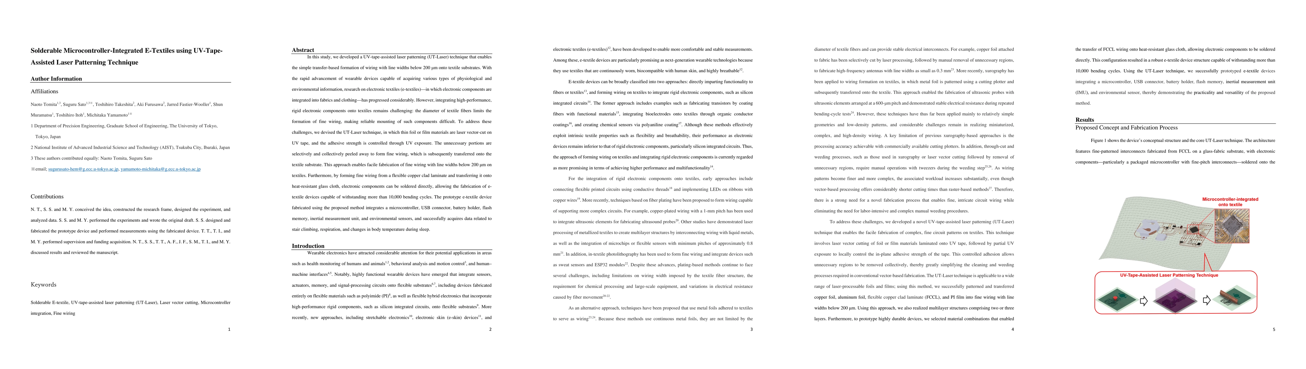
In this study, we developed a UV-tape-assisted laser patterning (UT-Laser) technique that enables the simple transfer-based formation of wiring with line widths below 200 $μ$m onto textile substrates. With the rapid advancement of wearable devices capable of acquiring various types of physiological and environmental information, research on electronic textiles (e-textiles)-in which electronic components are integrated into fabrics and clothing-has progressed considerably. However, integrating high-performance, rigid electronic components onto textiles remains challenging: the diameter of textile fibers limits the formation of fine wiring, making reliable mounting of such components difficult. To address these challenges, we devised the UT-Laser technique, in which thin foil or film materials are laser vector-cut on UV tape, and the adhesive strength is controlled through UV exposure. The unnecessary portions are selectively and collectively peeled away to form fine wiring, which is subsequently transferred onto the textile substrate. This approach enables facile fabrication of fine wiring with line widths below 200 $μ$m on textiles. Furthermore, by forming fine wiring from a flexible copper clad laminate and transferring it onto heat-resistant glass cloth, electronic components can be soldered directly, allowing the fabrication of e-textile devices capable of withstanding more than 10,000 bending cycles. The prototype e-textile device fabricated using the proposed method integrates a microcontroller, USB connector, battery holder, flash memory, inertial measurement unit, and environmental sensors, and successfully acquires data related to stair climbing, respiration, and changes in body temperature during sleep.
Key Findings, in focus
Seven facets of this paper, analysed and brought into focus by AI.
The technique allows high‑performance, rigid components to be integrated into flexible, breathable e‑textiles while leveraging existing PCB manufacturing infrastructure, thereby enabling durable, wearable devices that can endure >10,000 bending cycles
- Fine wiring with line widths below 200 µm was fabricated on glass cloth using aluminum, copper and FCCL foils
- Multilayer wiring structures were successfully created by repeating the UT‑Laser and transfer steps, enabling protective and interconnect layers
The technique allows high‑performance, rigid components to be integrated into flexible, breathable e‑textiles while leveraging existing PCB manufacturing infrastructure, thereby enabling durable, wearable devices that can endure >10,000 bending cycles
A novel UT‑Laser patterning and transfer method that produces sub‑200 µm fine wiring on textile substrates and enables direct soldering of rigid components using conventional PCB processes
Unlike prior flexible‑electronics methods that are limited to larger feature sizes or flexible components, this work combines UV‑tape laser patterning with transfer onto glass cloth, achieving fine, solderable wiring and multilayer structures on a breathable textile platform
- The current process does not support through‑vias, requiring separate connections for exposed terminals
- Adding more layers increases device thickness, potentially compromising the inherent softness of the textile
- Develop a method to create through‑vias within the transferred wiring
- Optimize layer thickness and material selection to maintain softness while preserving mechanical robustness
- Explore alternative textile substrates to broaden application scope
Discussion 0