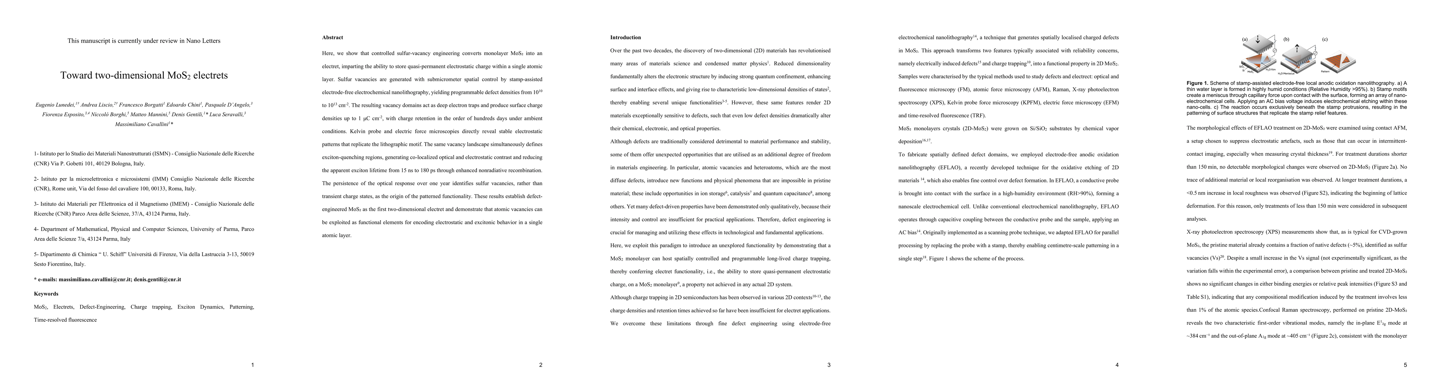
Here, we show that controlled sulfur vacancy engineering converts monolayer MoS2 into an electret, imparting the ability to store quasi-permanent electrostatic charge within a single atomic layer. Sulfur vacancies are generated with submicrometer spatial control by stamp-assisted electrode-free electrochemical nanolithography, yielding programmable defect densities from 10 10 to 10 13 1 cm-2. The resulting vacancy domains act as deep electron traps and produce surface charge densities up to 1 uCcm-2, with charge retention in the order of hundreds days under ambient conditions. Kelvin probe and electric force microscopies directly reveal stable electrostatic patterns that replicate the lithographic motif. The same vacancy landscape simultaneously defines exciton-quenching regions, generating co-localized optical and electrostatic contrast and reducing the apparent exciton lifetime from 15 ns to 180 ps through enhanced nonradiative recombination. The persistence of the optical response over one year identifies sulfur vacancies, rather than transient charge states, as the origin of the patterned functionality. These results establish defect-engineered MoS2 as the first two-dimensional electret and demonstrate that atomic vacancies can be exploited as functional elements for encoding electrostatic and excitonic behavior in a single atomic layer.
Discussion 0