The study utilized scanning tunneling microscopy (STM) to visualize the real-space charge landscape within Kondo lattices, specifically in URu2Si2 and SmB6, at atomic resolution.
Publication
Metrics
AI Quick Summary
This study uses a scanning tunneling microscope to reveal atomic-scale metallic conduction electron puddles in Kondo insulators, suggesting that defects disturb the Kondo screening cloud and may be responsible for observed 3D quantum oscillations. The technique could pave the way for atomic-scale charge sensors.
Quick Answers
What is "Visualizing the atomic-scale origin of metallic behavior in Kondo insulators" about?
This study uses a scanning tunneling microscope to reveal atomic-scale metallic conduction electron puddles in Kondo insulators, suggesting that defects disturb the Kondo screening cloud and may be responsible for observed 3D quantum oscillations. The technique could pave the way for atomic-scale charge sensors.
What methodology did the authors use?
The study utilized scanning tunneling microscopy (STM) to visualize the real-space charge landscape within Kondo lattices, specifically in URu2Si2 and SmB6, at atomic resolution. More in Methodology →
What are the key results?
Nanometer-scale puddles of metallic conduction electrons were discovered centered around uranium-site substitutions in URu2Si2 and samarium-site defects in SmB6. — These defects disturb the Kondo screening cloud, leaving a fingerprint of the metallic parent state. More in Key Results →
Why is this work significant?
This research provides insights into the atomic-scale origin of metallic behavior in Kondo insulators, which could lead to a better understanding of heavy-fermion systems and topological Kondo insulators. More in Significance →
What are the main limitations?
The study did not definitively rule out other explanations for the quantum oscillations in SmB6 besides Kondo-lattice defects. — The technique is limited to materials that can be studied with STM at atomic resolution. More in Limitations →
Abstract
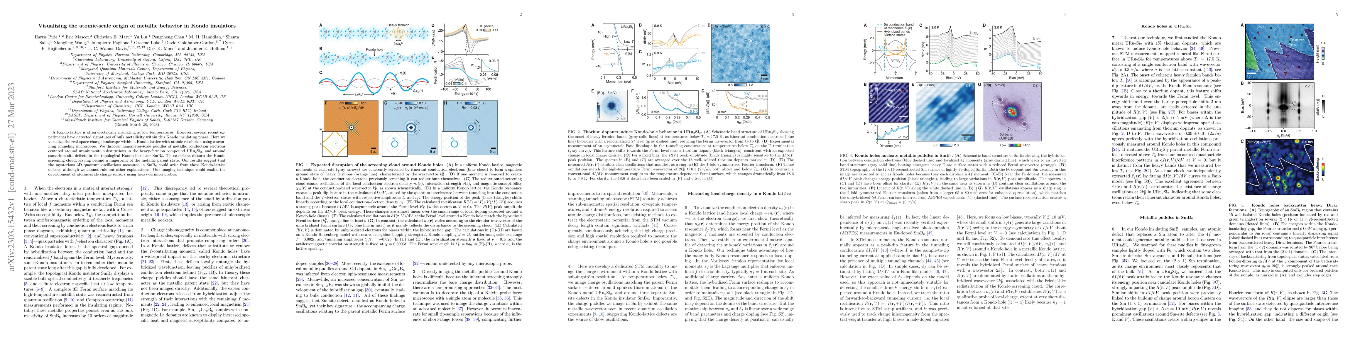
A Kondo lattice is often electrically insulating at low temperatures. However, several recent experiments have detected signatures of bulk metallicity within this Kondo insulating phase. Here we visualize the real-space charge landscape within a Kondo lattice with atomic resolution using a scanning tunneling microscope. We discover nanometer-scale puddles of metallic conduction electrons centered around uranium-site substitutions in the heavy-fermion compound URu$_2$Si$_2$, and around samarium-site defects in the topological Kondo insulator SmB$_6$. These defects disturb the Kondo screening cloud, leaving behind a fingerprint of the metallic parent state. Our results suggest that the mysterious 3D quantum oscillations measured in SmB$_6$ could arise from these Kondo-lattice defects, although we cannot rule out other explanations. Our imaging technique could enable the development of atomic-scale charge sensors using heavy-fermion probes.
Key Findings, in focus
Seven facets of this paper, analysed and brought into focus by AI.
This research provides insights into the atomic-scale origin of metallic behavior in Kondo insulators, which could lead to a better understanding of heavy-fermion systems and topological Kondo insulators.
- Nanometer-scale puddles of metallic conduction electrons were discovered centered around uranium-site substitutions in URu2Si2 and samarium-site defects in SmB6.
- These defects disturb the Kondo screening cloud, leaving a fingerprint of the metallic parent state.
- The results suggest that the 3D quantum oscillations in SmB6 could arise from these Kondo-lattice defects, although other explanations are not ruled out.
- The imaging technique could enable the development of atomic-scale charge sensors using heavy-fermion probes.
This research provides insights into the atomic-scale origin of metallic behavior in Kondo insulators, which could lead to a better understanding of heavy-fermion systems and topological Kondo insulators.
The development and application of STM to visualize and analyze the real-space charge landscape within Kondo lattices at atomic resolution.
This work is novel in directly visualizing metallic puddles around defects in Kondo insulators, providing a new perspective on the metallic behavior within these systems.
- The study did not definitively rule out other explanations for the quantum oscillations in SmB6 besides Kondo-lattice defects.
- The technique is limited to materials that can be studied with STM at atomic resolution.
- Further experiments could investigate other Kondo insulators to confirm if similar metallic puddles exist.
- Theoretical work could explore alternative explanations for the quantum oscillations observed.
Impact
Paper Details
Authors
PDF Preview
Key Terms
Citation Network
Current paper (gray), citations (green), references (blue)
Display is limited for performance on very large graphs.
Discussion 0