Publication
Metrics
AI Quick Summary
This paper introduces a waveguide-integrated, plasmonic enhanced graphene photodetector (GPD) with zero dark current, optimized for telecom wavelengths. The device achieves high responsivity and bandwidth, leveraging plasmonic effects to enhance light-graphene interaction and improve photovoltage generation.
Paper Preview
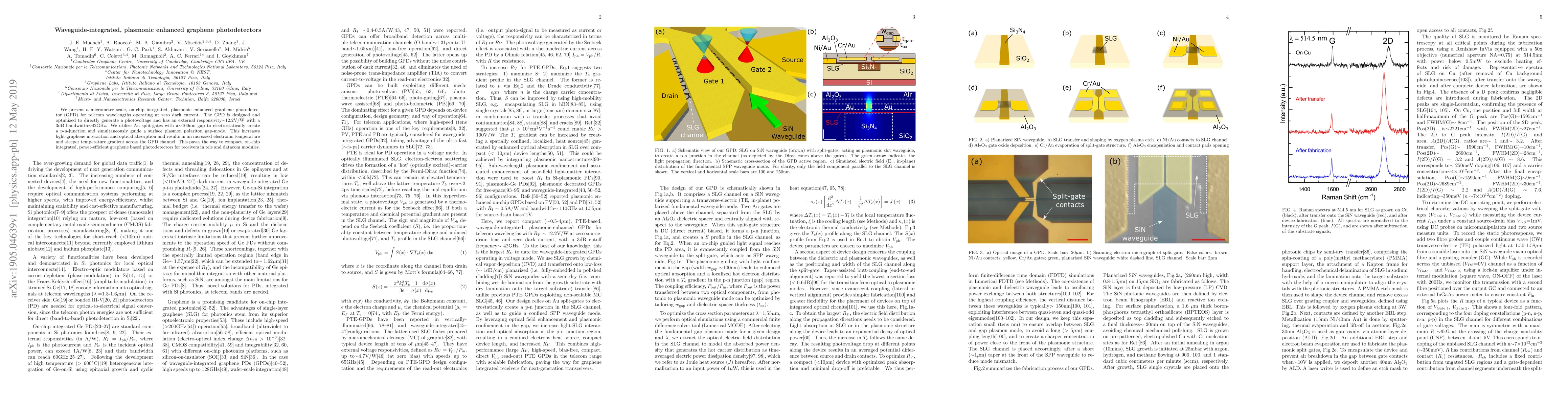
Abstract
We present a micrometer scale, on-chip integrated, plasmonic enhanced graphene photodetector (GPD) for telecom wavelengths operating at zero dark current. The GPD is designed and optimized to directly generate a photovoltage and has an external responsivity~12.2V/W with a 3dB bandwidth~42GHz. We utilize Au split-gates with a$\sim$100nm gap to electrostatically create a p-n-junction and simultaneously guide a surface plasmon polariton gap-mode. This increases light-graphene interaction and optical absorption and results in an increased electronic temperature and steeper temperature gradient across the GPD channel. This paves the way to compact, on-chip integrated, power-efficient graphene based photodetectors for receivers in tele and datacom modules
AI Key Findings
Get AI-generated insights about this paper's methodology, results, significance, and more — seven facets brought into focus.
Impact
Paper Details
Authors
PDF Preview
Key Terms
Citation Network
Current paper (gray), citations (green), references (blue)
Display is limited for performance on very large graphs.
Discussion 0