ArxivLens
A
Researcher

Abbes Tahraoui

6 papers on arXiv

6 arXiv Papers
126 Total Publications
Profile

Academic Profile

Name A. Tahraoui
Total Papers 126
Scholar Profile View on Semantic Scholar
Metrics

Statistics

6 arXiv Papers
126 Total Publications
Publications

Papers on arXiv

Thumbnail for Uniform large-area surface patterning achieved by metal dewetting for
  the top-down fabrication of GaN nanowire ensembles
arXiv
Uniform large-area surface patterning achieved by metal dewetting for the top-down fabrication of GaN nanowire ensembles

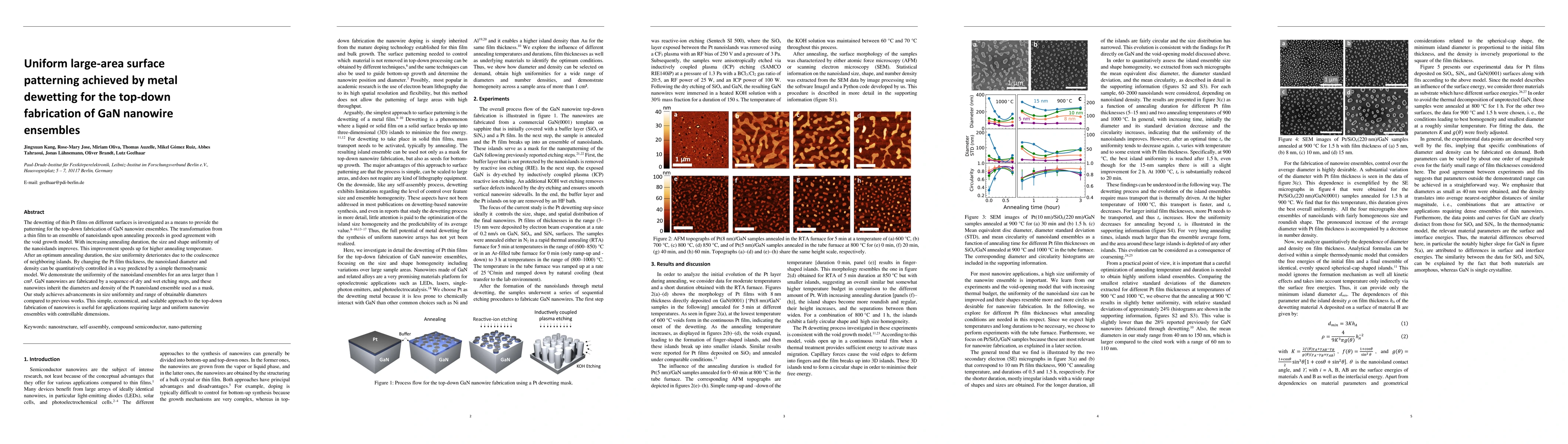
The dewetting of thin Pt films on different surfaces is investigated as a means to provide the patterning for the top-down fabrication of GaN nanowire ensembles. The transformation from a thin film ...

Thumbnail for A route for the top-down fabrication of ordered ultrathin GaN nanowires
arXiv
A route for the top-down fabrication of ordered ultrathin GaN nanowires

Ultrathin GaN nanowires (NWs) are attractive to maximize surface effects and as building block in high-frequency transistors. Here, we introduce a facile route for the top-down fabrication of ordere...

Thumbnail for GHz guided optomechanics in planar semiconductor microcavities
arXiv
GHz guided optomechanics in planar semiconductor microcavities

Hybrid opto, electro, and mechanical systems operating at several GHz offer extraordinary opportunities for the coherent control of opto-electronic excitations down to the quantum limit. We introduc...

Thumbnail for SnO/$\beta$-Ga2O3 vertical $pn$ heterojunction diodes
arXiv
SnO/$\beta$-Ga2O3 vertical $pn$ heterojunction diodes

Vertical $pn$ heterojunction diodes were prepared by plasma-assisted molecular beam epitaxy of unintentionally-doped $p$-type SnO layers with hole concentrations ranging from $p=10^{18}$ to $10^{19}...

Thumbnail for Selective-area van der Waals epitaxy of h-BN/graphene heterostructures
  via He$^{+}$ irradiation-induced defect-engineering in 2D substrates
arXiv
Selective-area van der Waals epitaxy of h-BN/graphene heterostructures via He$^{+}$ irradiation-induced defect-engineering in 2D substrates

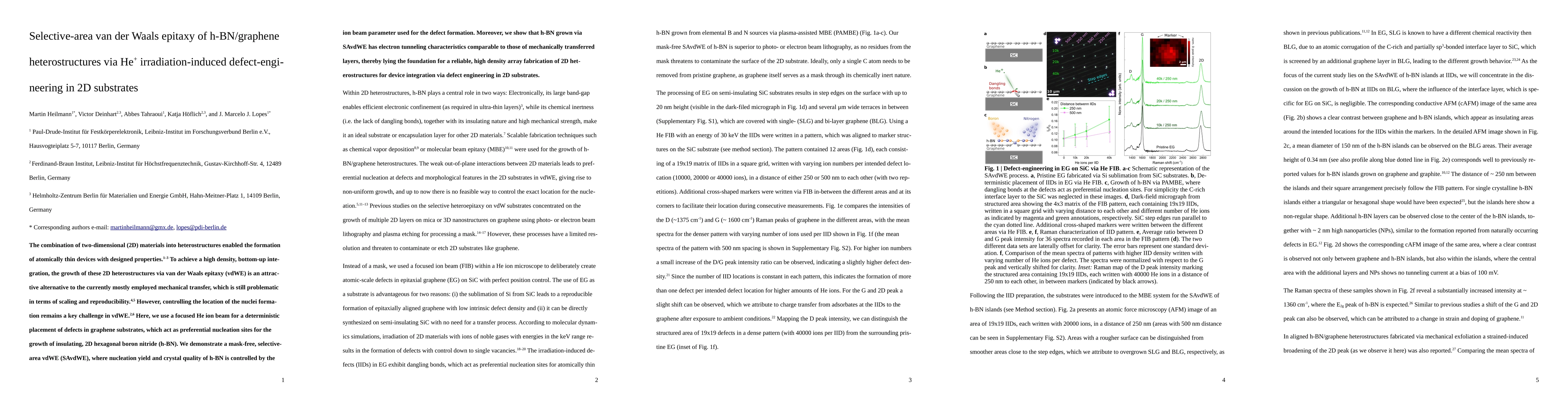
The combination of two-dimensional (2D) materials into heterostructures enabled the formation of atomically thin devices with designed properties. To achieve a high density, bottom-up integration, t...

Thumbnail for Electroluminescence and current-voltage measurements of single
  (In,Ga)N/GaN nanowire light-emitting diodes in the nanowire ensemble
arXiv
Electroluminescence and current-voltage measurements of single (In,Ga)N/GaN nanowire light-emitting diodes in the nanowire ensemble

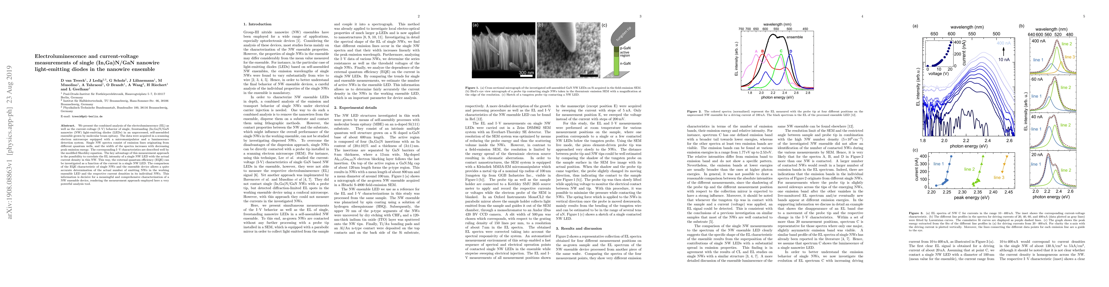
We present the combined analysis of the electroluminescence (EL) as well as the current-voltage (I-V) behavior of single, freestanding (In,Ga)N/GaN nanowire (NW) light-emitting diodes (LEDs) in an u...

This website uses cookies to ensure you get the best experience. Learn more