Academic Profile
Statistics
Similar Authors
Papers on arXiv
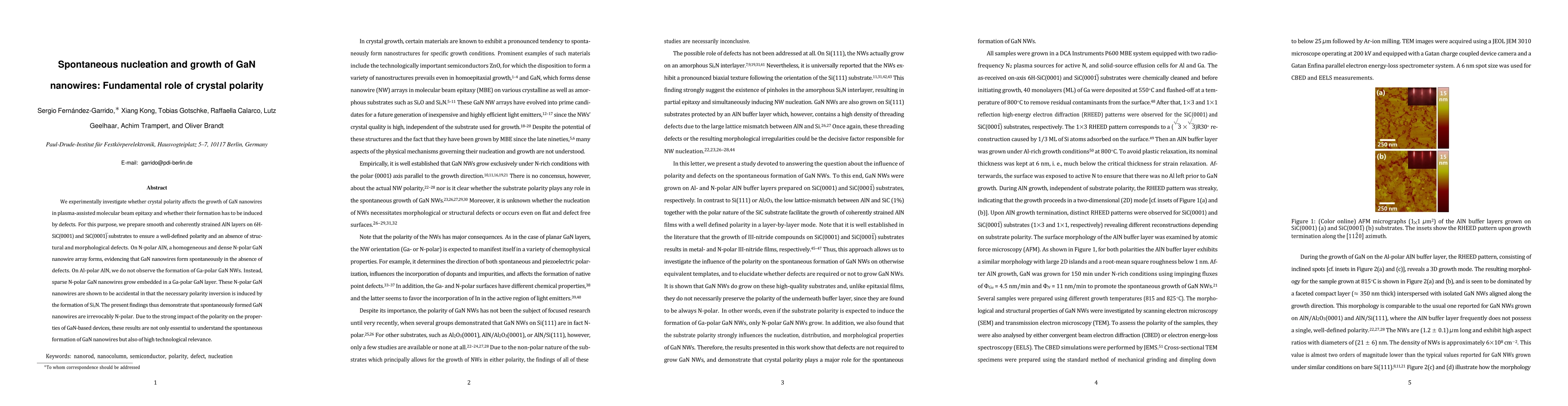
We experimentally investigate whether crystal polarity affects the growth of GaN nanowires in plasma-assisted molecular beam epitaxy and whether their formation has to be induced by defects. For thi...
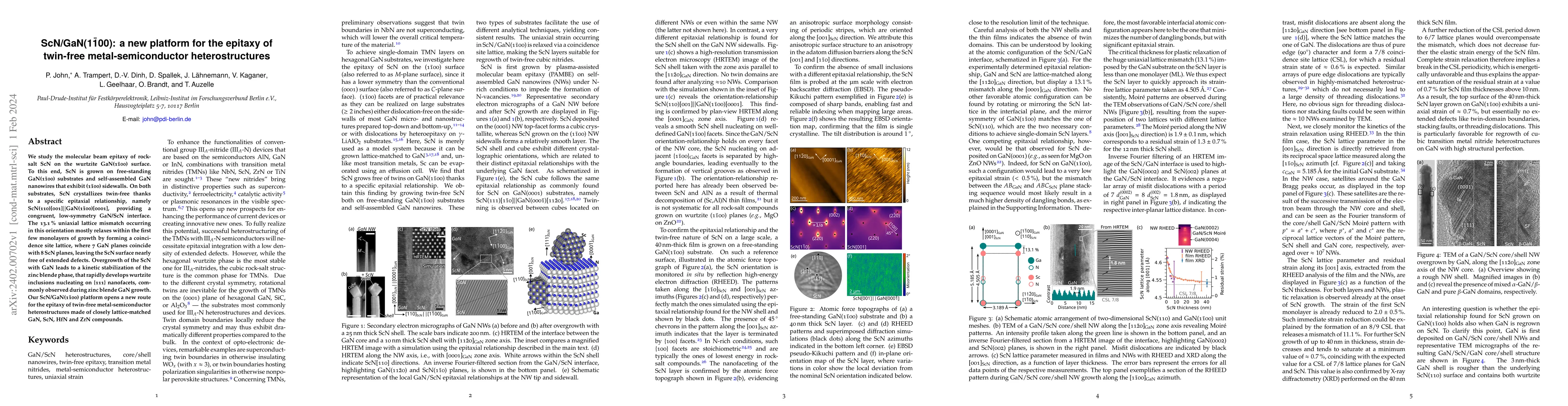
We study the molecular beam epitaxy of rock-salt ScN on the wurtzite GaN($1\bar{1}00$) surface. To this end, ScN is grown on free-standing GaN($1\bar{1}00$) substrates and self-assembled GaN nanowir...
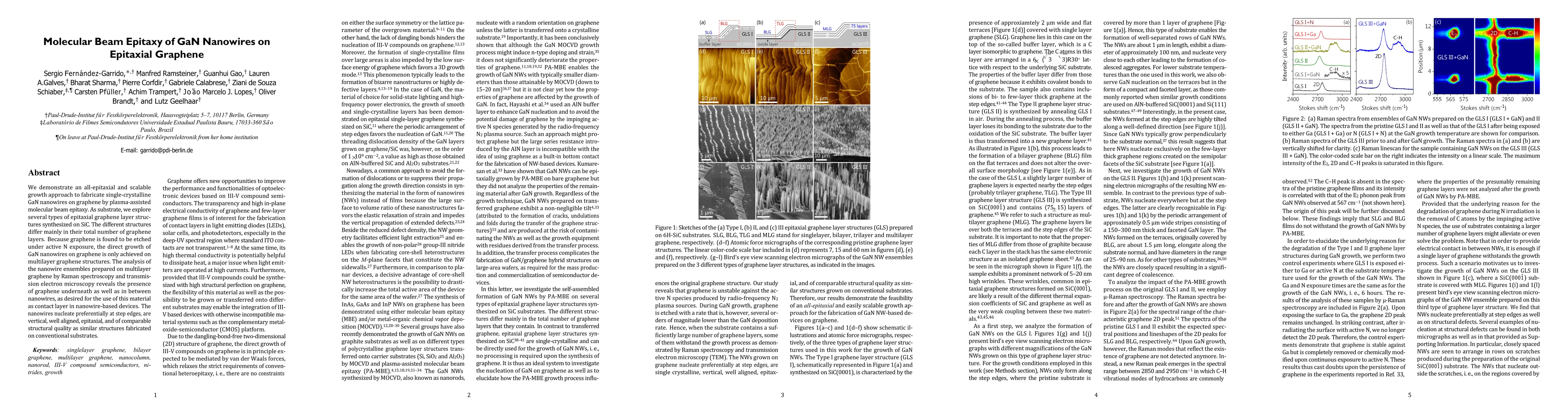
We demonstrate an all-epitaxial and scalable growth approach to fabricate single-crystalline GaN nanowires on graphene by plasma-assisted molecular beam epitaxy. As substrate, we explore several typ...
The realization of semiconductor structures with stable excitons at room temperature is crucial for the development of excitonics and polaritonics. Quantum confinement has commonly been employed for...
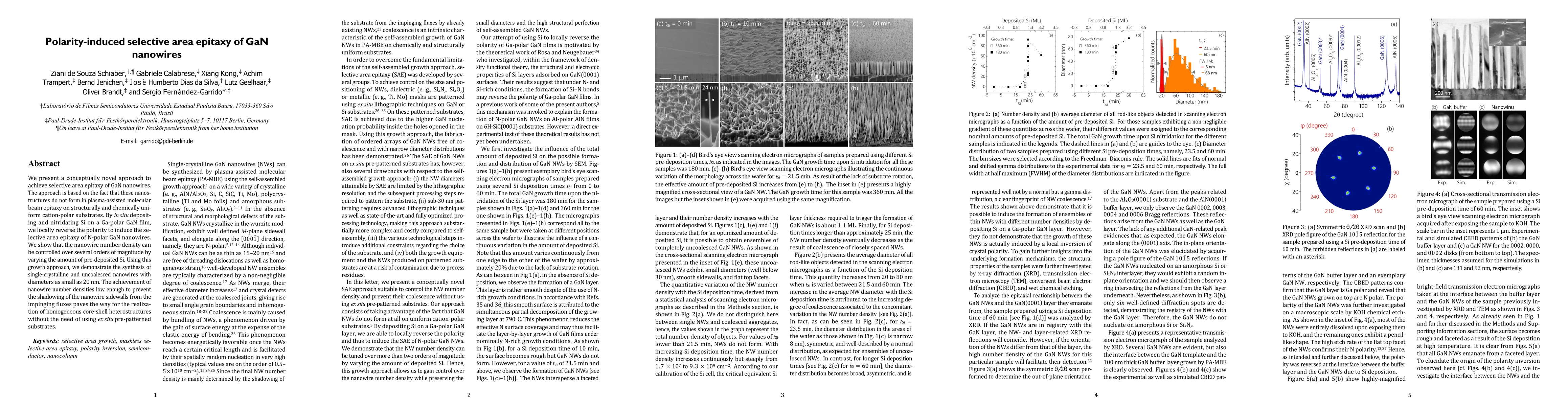
We present a conceptually novel approach to achieve selective area epitaxy of GaN nanowires. The approach is based on the fact that these nanostructures do not form in plasma-assisted molecular beam...
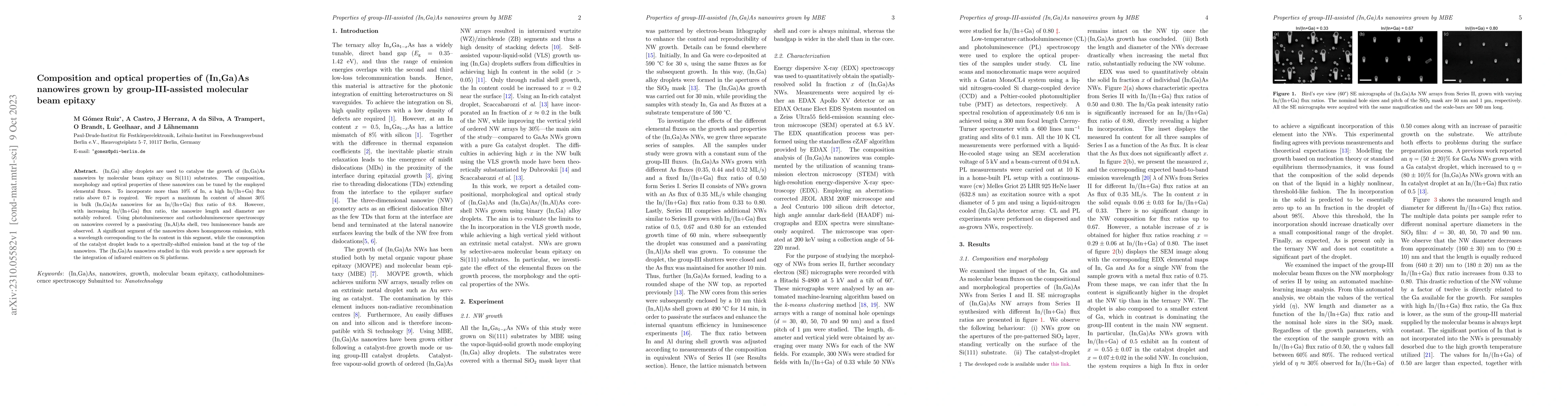
(In,Ga) alloy droplets are used to catalyse the growth of (In,Ga)As nanowires by molecular beam epitaxy on Si(111) substrates. The composition, morphology and optical properties of these nanowires c...
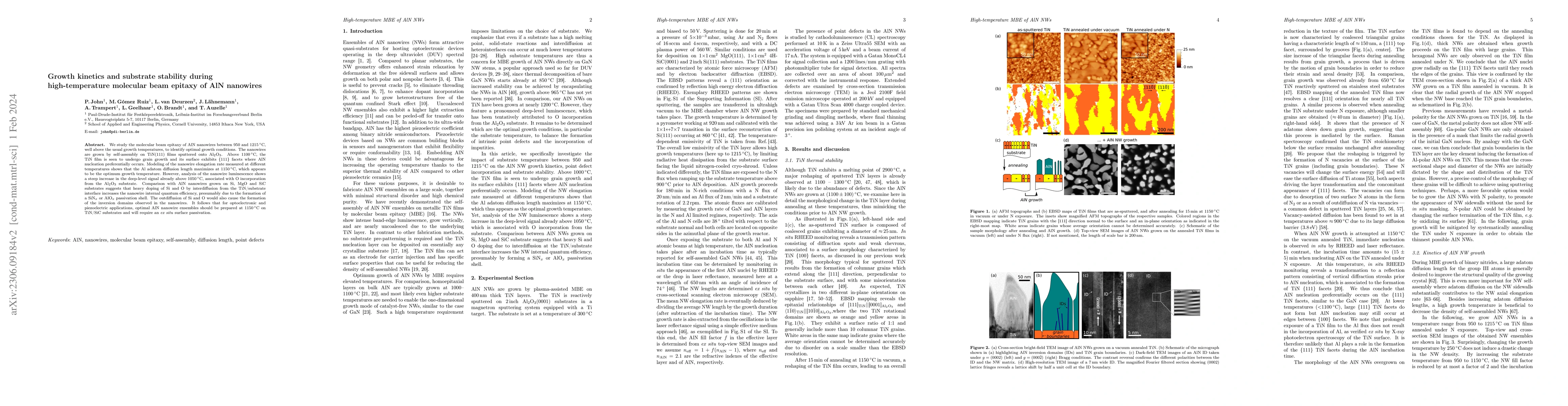
We study the molecular beam epitaxy of AlN nanowires between 950 and 1215 {\deg}C, well above the usual growth temperatures, to identify optimal growth conditions. The nanowires are grown by self-as...
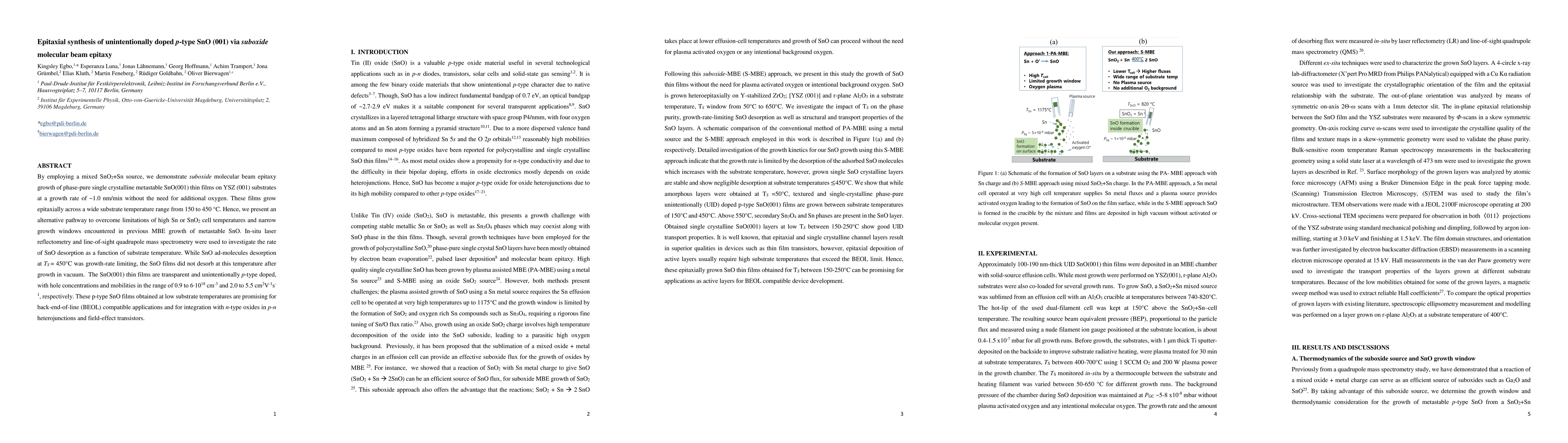
By employing a mixed SnO$_2$+Sn source, we demonstrate suboxide molecular beam epitaxy growth of phase-pure single crystalline metastable SnO(001) thin films at a growth rate of ~1.0nm/min without t...
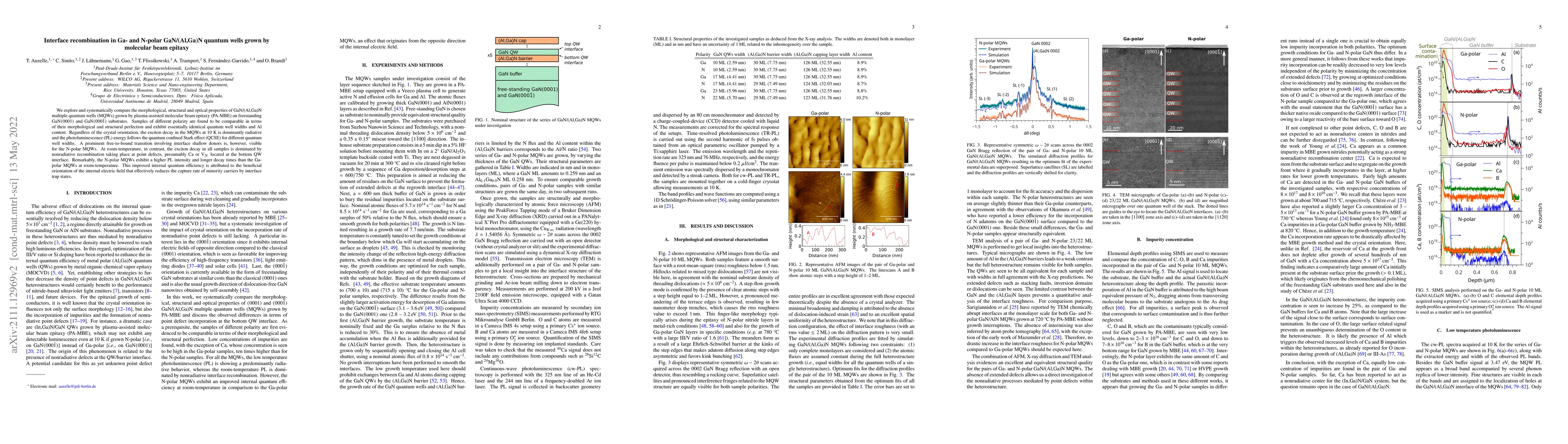
We explore and systematically compare the morphological, structural and optical properties of GaN/(Al,Ga)N multiple quantum wells (MQWs) grown by plasma-assisted molecular beam epitaxy (PA-MBE) on f...
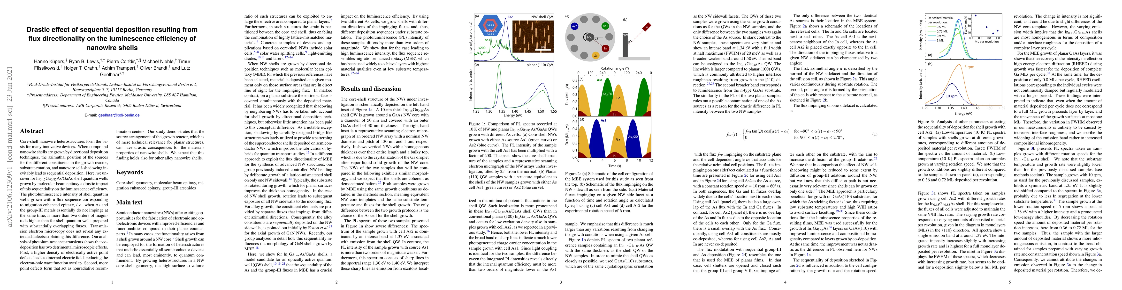
Core-shell nanowire heterostructures form the basis for many innovative devices. When compound nanowire shells are grown by directional deposition techniques, the azimuthal position of the sources f...
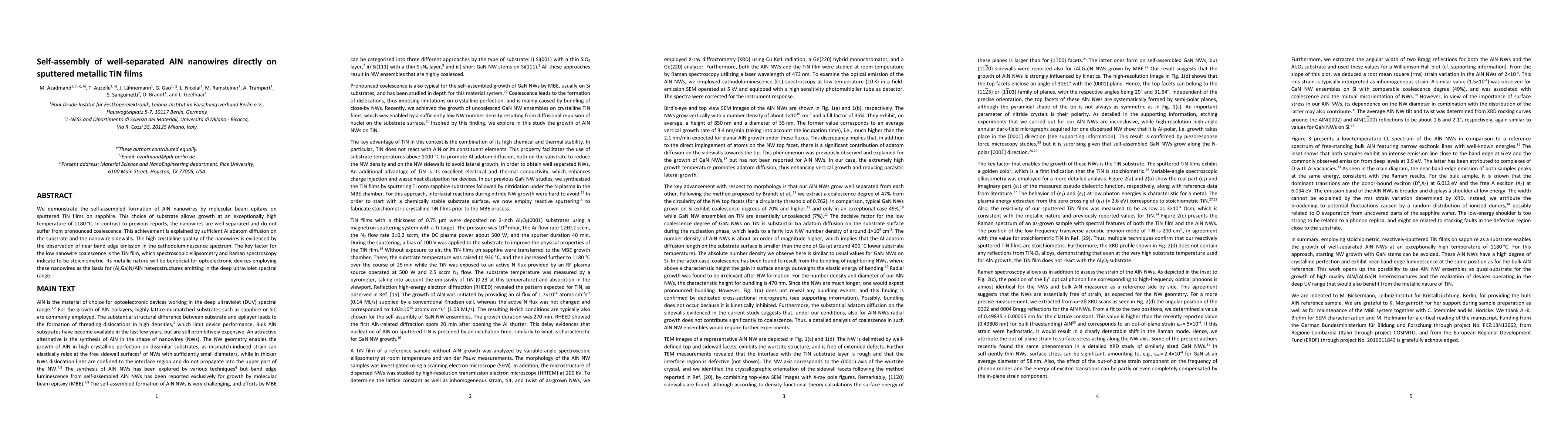
We demonstrate the self-assembled formation of AlN nanowires by molecular beam epitaxy on sputtered TiN films on sapphire. This choice of substrate allows growth at an exceptionally high temperature...
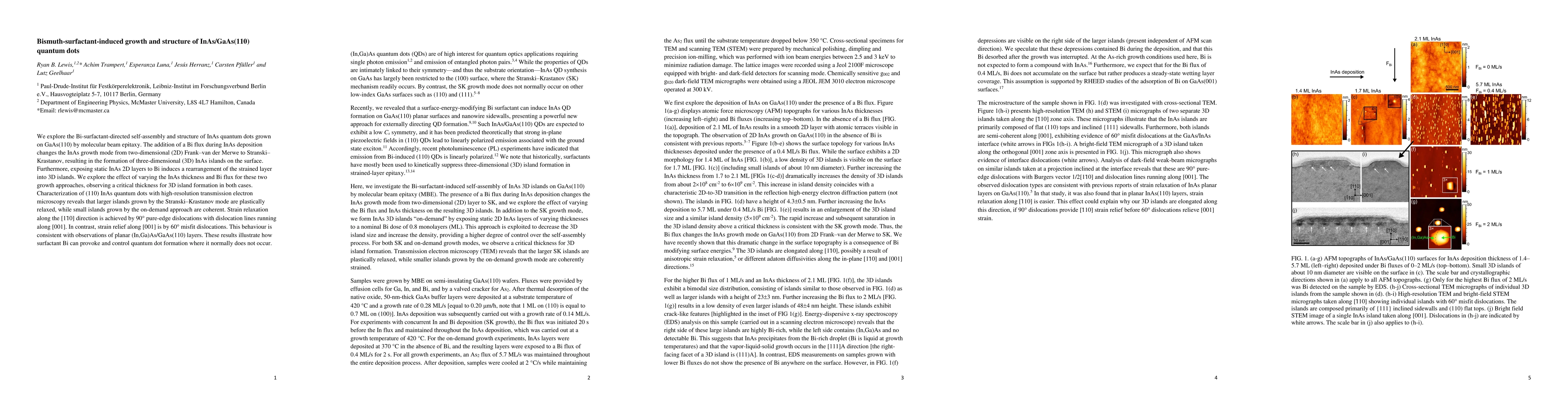
We explore the Bi-surfactant-directed self-assembly and structure of InAs quantum dots grown on GaAs(110) by molecular beam epitaxy. The addition of a Bi flux during InAs deposition changes the InAs...
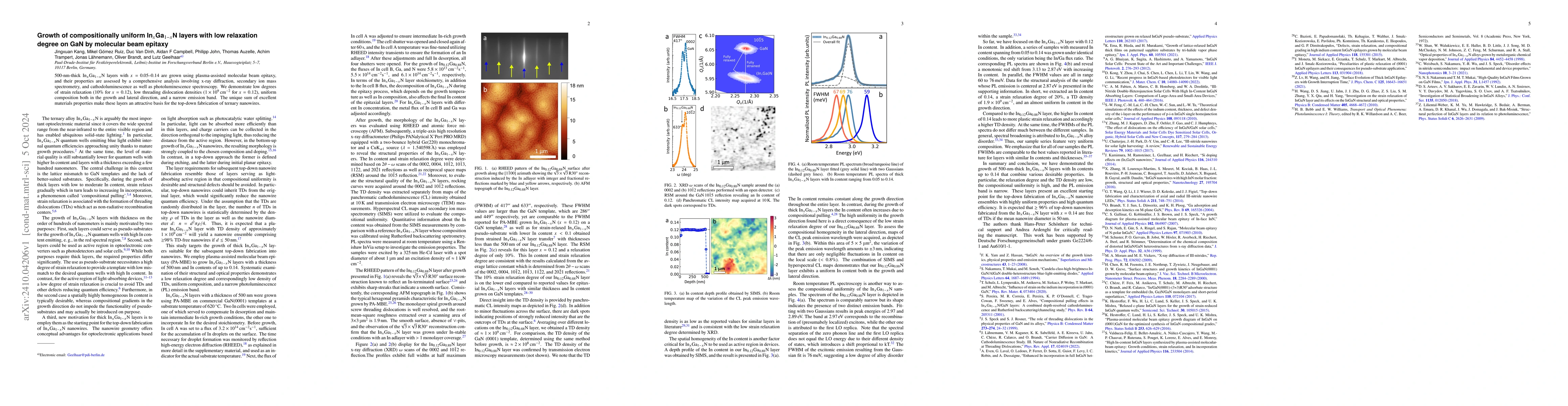
500-nm-thick $\mathrm{In}_{x}\mathrm{Ga}_{1-x}\mathrm{N}$ layers with $x=$ 0.05-0.14 are grown using plasma-assisted molecular beam epitaxy, and their properties are assessed by a comprehensive analys...
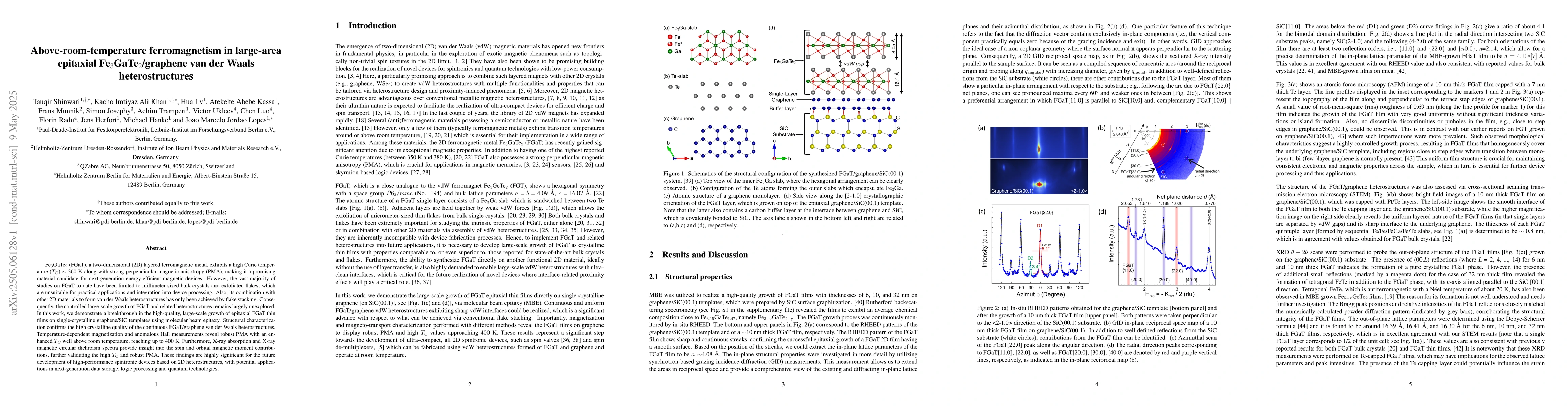
Fe3GaTe2 (FGaT), a two-dimensional (2D) layered ferromagnetic metal, exhibits a high Curie temperature (TC) ~ 360 K along with strong perpendicular magnetic anisotropy (PMA), making it a promising mat...
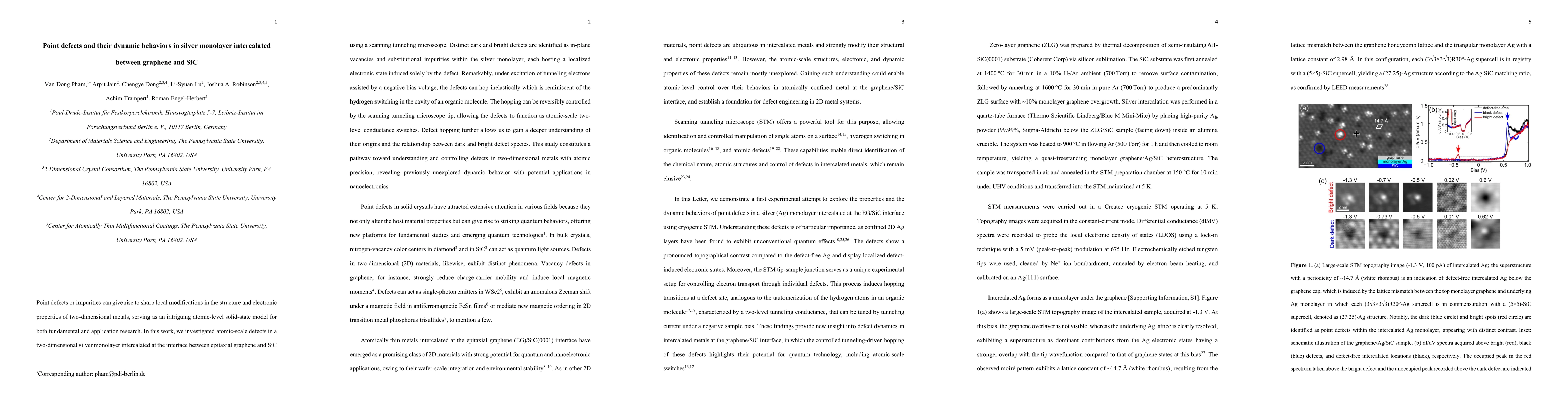
Point defects or impurities can give rise to sharp local modifications in the structure and electronic properties of two-dimensional metals, serving as an intriguing atomic-level solid-state model for...
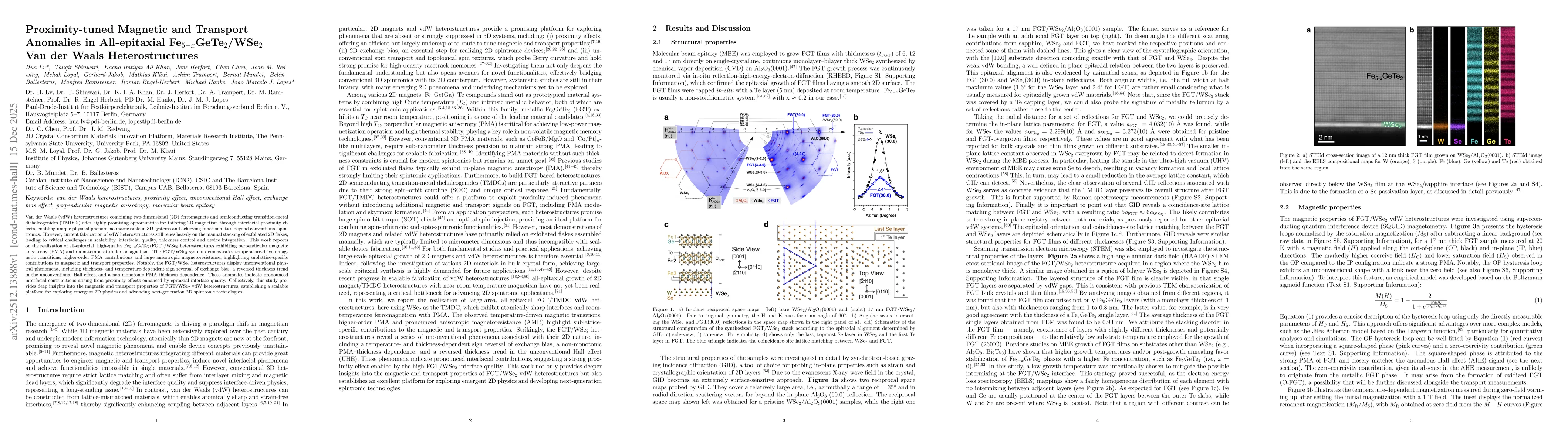
Van der Waals (vdW) heterostructures combining two-dimensional (2D) ferromagnets and semiconducting transition-metal dichalcogenides (TMDCs) offer highly promising opportunities for tailoring 2D magne...