This study reveals that crystal polarity significantly influences the spontaneous nucleation and growth of GaN nanowires in plasma-assisted molecular beam epitaxy, with N-polar nanowires forming naturally on N-polar AlN substrates, while Ga-polar nanowires do not form on Al-polar AlN substrates. These findings underscore the importance of polarity in the properties and technological applications of GaN-based devices.
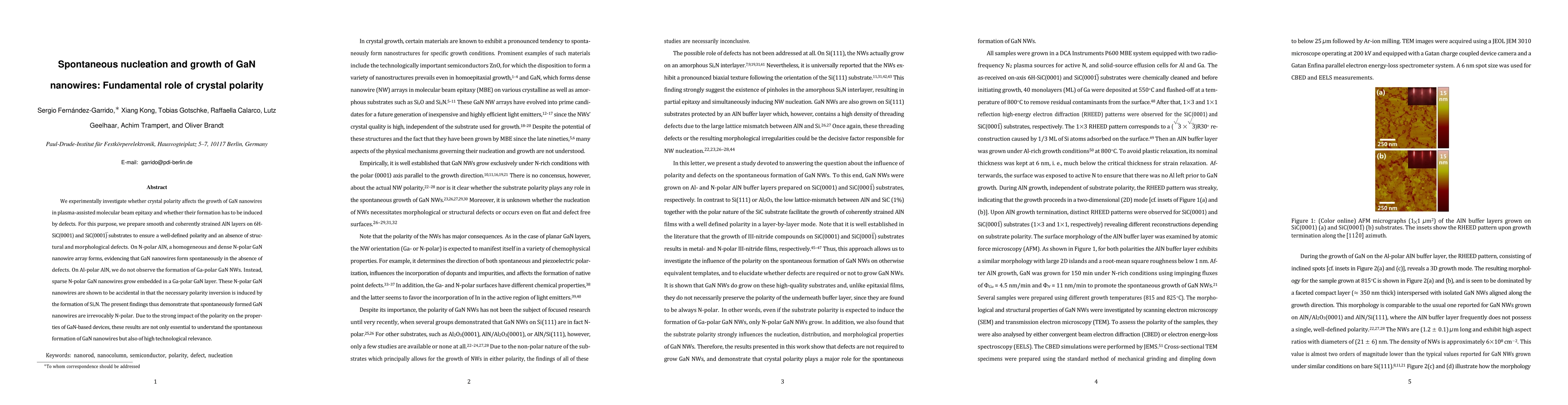
We experimentally investigate whether crystal polarity affects the growth of GaN nanowires in plasma-assisted molecular beam epitaxy and whether their formation has to be induced by defects. For this purpose, we prepare smooth and coherently strained AlN layers on 6H-SiC(0001) and SiC(000$\bar{1}$) substrates to ensure a well-defined polarity and an absence of structural and morphological defects. On N-polar AlN, a homogeneous and dense N-polar GaN nanowire array forms, evidencing that GaN nanowires form spontaneously in the absence of defects. On Al-polar AlN, we do not observe the formation of Ga-polar GaN NWs. Instead, sparse N-polar GaN nanowires grow embedded in a Ga-polar GaN layer. These N-polar GaN nanowires are shown to be accidental in that the necessary polarity inversion is induced by the formation of Si$_{x}$N. The present findings thus demonstrate that spontaneously formed GaN nanowires are irrevocably N-polar. Due to the strong impact of the polarity on the properties of GaN-based devices, these results are not only essential to understand the spontaneous formation of GaN nanowires but also of high technological relevance.
This graph shows how this paper is connected to other research. The current paper is shown in dark gray, papers that cite it are in green, and papers it references are in blue. You can:
• Hover over any node to see the paper title
• Click a node to view that paper's details
• Drag nodes to rearrange the graph
• Use the zoom controls (bottom right) to zoom in/out
Title | Authors | Year | Actions |
---|---|---|---|
Efficient coupling between photonic waveguides and III-nitride quantum emitters in the UV-visible spectral range
|
Md. Jawad Ul Islam, Mrinmoy Kundu, Nirmal Anand, S. Sadaf, Md Zunaid Baten
|
2024
|
View Paper |
Detection of an unintentional Si doping gradient in site-controlled GaN nanowires grown using a Si3N4 mask by spatially resolved cathodoluminescence and Raman spectroscopy
|
Mikel Gómez Ruiz, M. Brubaker, Kris A. Bertness, A. Roshko, H. Tornatzky, M. Ramsteiner, Oliver Brandt, J. Lähnemann
|
2024
|
View Paper |
Selective Area Epitaxy of GaN Nanostructures: MBE Growth and Morphological Analysis
|
Syed M. N. Hasan, Weicheng You, A. Ghosh, S. Sadaf, S. Arafin
|
2023
|
View Paper |
Influence of gallium surface saturation on GaN nanowire polytype selection during molecular-beam epitaxy
|
H. Lu, S. Moniri, C. Reese, S. Jeon, A. Katcher, T. Hill, Hui Deng, Rachel S. Goldman
|
2021
|
View Paper |
Recent Progress on Aluminum Gallium Nitride Deep Ultraviolet Lasers by Molecular Beam Epitaxy
|
Qihua Zhang, Xue Yin, Songrui Zhao
|
2021
|
View Paper |
Dual-wavelength visible photodetector based on vertical (In,Ga)N nanowires grown by molecular beam epitaxy
|
Jianya Zhang, Min Zhou, Dongmin Wu, L. Bian, Yukun Zhao, H. Qin, Wenxian Yang, Yuanyuan Wu, Z. Xing, Shulong Lu
|
2021
|
View Paper |
Influence of Si Substrate Preparation Procedure on Polarity of Self-Assembled GaN Nanowires on Si(111): Kelvin Probe Force Microscopy Studies
|
M. Sobanska, N. Garro, K. Klosek, A. Cros, Z. Zytkiewicz
|
2020
|
View Paper |
Detaching (In,Ga)N Nanowire Films for Devices Requiring High Flexibility and Transmittance
|
Yukun Zhao, Z. Xing, L. Geelhaar, Jianya Zhang, Wenxian Yang, T. Auzelle, Yuanyuan Wu, L. Bian, Shulong Lu
|
2020
|
View Paper |
Small-angle X-ray scattering from GaN nanowires on Si(111): facet truncation rods, facet roughness and Porod’s law
|
V. Kaganer, O. Konovalov, S. Fern'andez-Garrido
|
2020
|
View Paper |
Crystallographic polarity measurements in two-terminal GaN nanowire devices by lateral piezoresponse force microscopy
|
M. Brubaker, A. Roshko, S. Berweger, P. Blanchard, Charles A. E. Little, T. Harvey, N. Sanford, K. Bertness
|
2020
|
View Paper |
Eutectic Formation, V/III Ratio, and Controlled Polarity Inversion in Nitrides on Silicon
|
A. Roshko, M. Brubaker, P. Blanchard, T. Harvey, K. Bertness
|
2020
|
View Paper |
Titanium Carbide MXene Nucleation Layer for Epitaxial Growth of High-Quality GaN Nanowires on Amorphous Substrates.
|
Aditya Prabaswara, Hyunho Kim, J. Min, Ram Chandra Subedi, D. Anjum, B. Davaasuren, Kalani Moore, M. Conroy, S. Mitra, I. Roqan, T. Ng, H. Alshareef, B. Ooi
|
2020
|
View Paper |
An electrically pumped surface-emitting semiconductor green laser
|
Y. Ra, R. Rashid, Xianhe Liu, S. Sadaf, Kishwar Mashooq, Z. Mi
|
2020
|
View Paper |
The influence of an AlN seeding layer on nucleation of self-assembled GaN nanowires on silicon substrates
|
Yao-zheng Wu, B. Liu, Zhenhua Li, T. Tao, Z. Xie, Ke Wang, X. Xiu, Dunjun Chen, Hai Lu, Rong Zhang, Youdou Zheng
|
2019
|
View Paper |
Self‐Assembly of Well‐Separated AlN Nanowires Directly on Sputtered Metallic TiN Films
|
M. Azadmand, T. Auzelle, J. Lähnemann, G. Gao, Lars Nicolai, M. Ramsteiner, A. Trampert, S. Sanguinetti, O. Brandt, L. Geelhaar
|
2019
|
View Paper |
Role of Ga Surface Diffusion in the Elongation Mechanism and Optical Properties of Catalyst-Free GaN Nanowires Grown by Molecular Beam Epitaxy.
|
M. Gruart, G. Jacopin, B. Daudin
|
2019
|
View Paper |
The role of Si in GaN/AlN/Si(111) plasma assisted molecular beam epitaxy: polarity and inversion
|
A. Roshko, M. Brubaker, P. Blanchard, T. Harvey, K. Bertness
|
2019
|
View Paper |
Effects of ultrathin AlN prelayers on the spontaneous growth of GaN nanowires by plasma assisted molecular beam epitaxy
|
S. Eftychis, J. E. Kruse, K. Tsagaraki, T. Koukoula, T. Kehagias, P. Komninou, A. Georgakilas
|
2019
|
View Paper |
Absence of quantum-confined Stark effect in GaN quantum disks embedded in (Al,Ga)N nanowires grown by molecular beam epitaxy.
|
C. Sinito, P. Corfdir, C. Pfüller, G. Gao, Javier Bartolomé Vílchez, S. Koelling, Alfonso Rodil Doblado, U. Jahn, J. Lähnemann, T. Auzelle, J. K. Zettler, T. Flissikowski, P. Koenraad, H. Grahn, L. Geelhaar, S. Fernández-Garrido, O. Brandt
|
2019
|
View Paper |
Gold-assisted growth of oxide bases underneath dewetted gold nanoparticles
|
Anchao Yi, Fang Liu, D. Xie, M. Wen, G. Zhu
|
2019
|
View Paper |
The Role of Polarity in Nonplanar Semiconductor Nanostructures.
|
M. de la Mata, R. Zamani, Sara Martí-Sánchez, M. Eickhoff, Q. Xiong, A. Fontcuberta i Morral, P. Caroff, J. Arbiol
|
2019
|
View Paper |
Polarity conversion of GaN nanowires grown by plasma-assisted molecular beam epitaxy
|
Alexandre Concordel, G. Jacopin, B. Gayral, N. Garro, A. Cros, J. Rouviere, B. Daudin
|
2019
|
View Paper |
Interfacial reactions during the molecular beam epitaxy of GaN nanowires on Ti/Al2O3
|
Gabriele Calabrese, Guanhui Gao, D. V. Treeck, P. Corfdir, C. Sinito, T. Auzelle, A. Trampert, L. Geelhaar, Oliver Brandt, S. Fernández-Garrido
|
2019
|
View Paper |
GaN nanowires on Si (111) substrates via molecular beam epitaxy: growth, electronic and optical properties
|
A. Bolshakov, V. Fedorov, G. Sapunov, A. Mozharov, L. N. Dvoreckaia, K. Shugurov, V. Shkoldin, I. Shtrom, M. Mukhin, G. Cirlin, I. Mukhin
|
2018
|
View Paper |
Tapering-induced enhancement of light extraction efficiency of nanowire deep ultraviolet LED by theoretical simulations
|
Ronghui Lin, Sergio Valdes Galan, Haiding Sun, Ya-Wen Hu, M. Alias, B. Janjua, T. Ng, B. Ooi, Xiaohang Li
|
2018
|
View Paper |
Growth of GaN nanowire ensembles in molecular beam epitaxy: Overcoming the limitations of their spontaneous formation
|
J. K. Zettler
|
2018
|
View Paper |
Plasma-assisted molecular beam epitaxy of GaN nanowires on epitaxial single-layer graphene
|
S. Fernández-Garrido, M. Ramsteiner, Lauren A. Galves, C. Sinito, P. Corfdir, Ziani de Souza Schiaber, J. Lopes, L. Geelhaar, O. Brandt
|
2018
|
View Paper |
Correlated Chemical and Electrically Active Dopant Analysis in Catalyst-Free Si-Doped InAs Nanowires.
|
J. Becker, M. Hill, M. Sonner, J. Treu, M. Döblinger, A. Hirler, H. Riedl, J. Finley, L. Lauhon, G. Koblmueller
|
2018
|
View Paper |
Arrangement of GaN nanowires on Si(001) substrates studied by X-ray diffraction: Importance of silicon nitride interlayer
|
A. Wierzbicka, G. Tchutchulashvili, M. Sobanska, K. Klosek, R. Minikayev, J. Domagała, J. Borysiuk, Z. Zytkiewicz
|
2017
|
View Paper |
Anomalous Structural Variations in III-Nitride Nanowire Heterostructures and Their Corresponding Optical Properties
|
S. Woo
|
2017
|
View Paper |
Control of ZnO nanowire growth and optical properties in a vapor deposition process
|
Nannan Bi, Lei Zhang, Q. Zheng, F. Zhuge, Jiu-Yan Li, Xuan P. A. Gao, Juan Du
|
2017
|
View Paper |
Molecular Beam Epitaxy of GaN Nanowires on Epitaxial Graphene.
|
S. Fernández-Garrido, M. Ramsteiner, G. Gao, Lauren A. Galves, B. Sharma, P. Corfdir, G. Calabrese, Ziani de Souza Schiaber, C. Pfüller, A. Trampert, J. Lopes, O. Brandt, L. Geelhaar
|
2017
|
View Paper |
Self-planarized quantum-disks-in-nanowires ultraviolet-B emitters utilizing pendeo-epitaxy.
|
B. Janjua, Haiding Sun, Chao Zhao, D. H. Anjum, Feng Wu, A. A. Alhamoud, A. A. Alhamoud, Xiaohang Li, A. Albadri, A. Alyamani, M. El-Desouki, T. Ng, Boon S. Ooi
|
2017
|
View Paper |
Polarity Control of Heteroepitaxial GaN Nanowires on Diamond.
|
M. Hetzl, Max Kraut, T. Hoffmann, M. Stutzmann
|
2017
|
View Paper |
Nitride-based Quantum-Confined Structures for Ultraviolet-Visible Optical Devices on Silicon Substrates
|
B. Janjua
|
2017
|
View Paper |
The effect of the three-dimensional strain variation on the emission properties of light-emitting diodes based on (In,Ga)N/GaN nanowires
|
M. Musolino, F. Sacconi, A. Tahraoui, F. Panetta, C. D. Santi, M. Meneghini, E. Zanoni, L. Geelhaar
|
2017
|
View Paper |
Comparison of convergent beam electron diffraction and annular bright field atomic imaging for GaN polarity determination
|
A. Roshko, M. Brubaker, P. Blanchard, K. Bertness, T. Harvey, R. Geiss, I. Levin
|
2017
|
View Paper |
Direct Imaging of Dopant Distribution in Polycrystalline ZnO Films.
|
Fanni Lorenzo, A. Aebersold, M. Morales-Masis, M. Ledinský, S. Escrig, A. Vetushka, D. Alexander, A. Hessler-Wyser, A. Fejfar, C. Hébert, S. Nicolay, C. Ballif
|
2017
|
View Paper |
Polarity-Induced Selective Area Epitaxy of GaN Nanowires.
|
Ziani de Souza Schiaber, G. Calabrese, X. Kong, A. Trampert, B. Jenichen, J. H. Dias da Silva, L. Geelhaar, O. Brandt, S. Fernández-Garrido
|
2017
|
View Paper |
GaN quantum dot polarity determination by X-ray photoelectron diffraction
|
O. Romanyuk, I. Bartoš, J. Brault, P. Mierry, T. Paskova, P. Jiříček
|
2016
|
View Paper |
Molecular dynamics simulation analysis of ion irradiation induced defects in an amorphous silicon dioxide nanowire
|
M. Nourazar
|
2016
|
View Paper |
Polarity in GaN and ZnO: Theory, measurement, growth, and devices
|
J. Zúñiga-Pérez, V. Consonni, L. Lymperakis, X. Kong, A. Trampert, S. Fernández-Garrido, O. Brandt, H. Renevier, S. Keller, K. Hestroffer, M. R. Wagner, J. Reparaz, F. Akyol, S. Rajan, S. Rennesson, T. Palacios, G. Feuillet
|
2016
|
View Paper |
Spontaneous growth of GaN nanowire nuclei on N- and Al-polar AlN: A piezoresponse force microscopy study of crystallographic polarity
|
M. Brubaker, A. Roshko, P. Blanchard, T. Harvey, N. Sanford, K. Bertness
|
2016
|
View Paper |
Reprint of: GaN nanowires on diamond
|
M. Hetzl, F. Schuster, Andrea Winnerl, Saskia Weiszer, M. Stutzmann
|
2016
|
View Paper |
Material characteristics of self-assembled mushroom-like InGaN nanocolumns
|
Qiming Chen, C. Yan, Y. Qu
|
2016
|
View Paper |
Wetting behavior of water on silicon carbide polar surfaces.
|
W. Zhong, Y. F. Huang, D. Gan, J. Y. Xu, H. Li, G. Wang, S. Meng, X. L. Chen
|
2016
|
View Paper |
Atomic‐Scale Origin of Long‐Term Stability and High Performance of p‐GaN Nanowire Arrays for Photocatalytic Overall Pure Water Splitting
|
Golam Kibria, R. Qiao, Wanli Yang, I. Boukahil, Xianghua Kong, Xianghua Kong, F. Chowdhury, Michel Trudeau, W. Ji, Hong Guo, F. J. Himpsel, L. Vayssieres, Z. Mi
|
2016
|
View Paper |
GaN nanowires on diamond
|
M. Hetzl, F. Schuster, Andrea Winnerl, Saskia Weiszer, M. Stutzmann
|
2016
|
View Paper |
Selective-area growth of GaN nanowires on SiO2-masked Si (111) substrates by molecular beam epitaxy
|
J. Kruse, L. Lymperakis, S. Eftychis, A. Adikimenakis, G. Doundoulakis, K. Tsagaraki, M. Androulidaki, A. Olziersky, P. Dimitrakis, V. Ioannou-Sougleridis, P. Normand, T. Koukoula, T. Kehagias, P. Komninou, G. Konstantinidis, A. Georgakilas
|
2016
|
View Paper |
Corrigendum: Self-induced growth of vertical GaN nanowires on silica (2015 Nanotechnology 27 135602)
|
V. Kumaresan, L. Largeau, F. Oehler, H. Zhang, O. Mauguin, F. Glas, N. Gogneau, M. Tchernycheva, J. Harmand
|
2016
|
View Paper |
Nucleation, Growth, and Bundling of GaN Nanowires in Molecular Beam Epitaxy: Disentangling the Origin of Nanowire Coalescence.
|
V. Kaganer, S. Fernández-Garrido, P. Doğan, K. Sabelfeld, O. Brandt
|
2016
|
View Paper |
The hydride vapor phase epitaxy of GaN on silicon covered by nanostructures
|
U. Jahn, M. Musolino, J. Lähnemann, P. Doğan, S. F. Garrido, J. F. Wang, K. Xu, D. Cai, L. Bian, X. Gong, H. Yang
|
2016
|
View Paper |
Comprehensive investigation on the correlation of growth, structural and optical properties of GaN nanowires grown on Si(111) substrates by plasma assisted molecular beam epitaxy technique
|
R. Sarkar, R. Fandan, Krista R. Khiangte, S. Chouksey, A. M. Josheph, S. Das, S. Ganguly, D. Saha, A. Laha
|
2016
|
View Paper |
Self-induced growth of vertical GaN nanowires on silica
|
V. Kumaresan, L. Largeau, F. Oehler, H. Zhang, O. Mauguin, F. Glas, N. Gogneau, M. Tchernycheva, J. Harmand
|
2016
|
View Paper |
Molecular beam epitaxy of single crystalline GaN nanowires on a flexible Ti foil
|
G. Calabrese, P. Corfdir, G. Gao, C. Pfuller, A. Trampert, O. Brandt, L. Geelhaar, S. Fern'andez-Garrido
|
2016
|
View Paper |
Early stages of plasma induced nitridation of Si (111) surface and study of interfacial band alignment
|
S. Shetty, S. M. Shivaprasad
|
2016
|
View Paper |
Polarity-Controlled GaN/AlN Nucleation Layers for Selective-Area Growth of GaN Nanowire Arrays on Si(111) Substrates by Molecular Beam Epitaxy
|
M. Brubaker, S. Duff, T. Harvey, P. Blanchard, A. Roshko, A. Sanders, N. Sanford, K. Bertness
|
2016
|
View Paper |
Lattice-Polarity-Driven Epitaxy of Hexagonal Semiconductor Nanowires.
|
Ping Wang, Ying Yuan, Chao Zhao, Xinqiang Wang, Xiantong Zheng, X. Rong, Tao Wang, B. Sheng, Qingxiao Wang, Yongqiang Zhang, L. Bian, Xuelin Yang, Fujun Xu, Zhixin Qin, Xin-Zheng Li, Xi-xiang Zhang, B. Shen
|
2016
|
View Paper |
GaN/AlN nanowires : nucleation, polarity and quantum heterostructures
|
T. Auzelle
|
2015
|
View Paper |
III-Nitride nanowire optoelectronics
|
Songrui Zhao, H. Nguyen, M. Kibria, Z. Mi
|
2015
|
View Paper |
Comparison of the Luminous Efficiencies of Ga- and N-Polar In x Ga 1 -x N /In y Ga 1 -y N Quantum Wells Grown by Plasma-Assisted Molecular Beam Epitaxy
|
S. Fern'andez-Garrido, J. Lahnemann, C. Hauswald, M. Korytov, M. Albrecht, C. Chèze, C. Skierbiszewski, O. Brandt
|
2015
|
View Paper |
Atomic scale characterizationof semiconductor non-planar nanostructures
|
María de la Mata Fernández
|
2015
|
View Paper |
Polarity of GaN with polar {0001} and semipolar , , orientations by x-ray photoelectron diffraction
|
O. Romanyuk, P. Jiříček, T. Paskova, I. Bartoš
|
2015
|
View Paper |
Spontaneous shape transition of thin films into ZnO nanowires with high structural and optical quality.
|
S. Guillemin, E. Sarigiannidou, E. Appert, F. Donatini, G. Renou, G. Brémond, V. Consonni
|
2015
|
View Paper |
MBE Growth of AlN Nanowires on Si Substrates by Aluminizing Nucleation
|
Y. E, Z. Hao, Jiadong Yu, Chao Wu, Ru-Shi Liu, Lai Wang, B. Xiong, Jian Wang, Yanjun Han, Changzheng Sun, Yi Luo
|
2015
|
View Paper |
Alternating-Current InGaN/GaN Tunnel Junction Nanowire White-Light Emitting Diodes.
|
S. Sadaf, Y. Ra, Hieu. P. T. Nguyen, M. Djavid, Z. Mi
|
2015
|
View Paper |
Assessment of Polarity in GaN Self-Assembled Nanowires by Electrical Force Microscopy.
|
A. Minj, A. Cros, N. Garro, J. Colchero, T. Auzelle, B. Daudin
|
2015
|
View Paper |
The influence of AlN buffer over the polarity and the nucleation of self-organized GaN nanowires
|
T. Auzelle, B. Haas, A. Minj, C. Bougerol, J. Rouviere, A. Cros, J. Colchero, B. Daudin
|
2015
|
View Paper |
Dynamics of free and bound excitons in GaN nanowires
|
C. Hauswald
|
2015
|
View Paper |
High efficiency AlGaN deep ultraviolet light emitting diodes on silicon
|
Z. Mi, Songrui Zhao, A. Connie, Mohammad Hadi Tavakoli Dastjerdi
|
2015
|
View Paper |
Monitoring the formation of nanowires by line-of-sight quadrupole mass spectrometry: a comprehensive description of the temporal evolution of GaN nanowire ensembles.
|
S. Fernández-Garrido, J. K. Zettler, L. Geelhaar, O. Brandt
|
2015
|
View Paper |
Aluminum nitride nanowire light emitting diodes: Breaking the fundamental bottleneck of deep ultraviolet light sources
|
Songrui Zhao, A. Connie, M. Dastjerdi, Xianghua Kong, Qi Wang, M. Djavid, S. Sadaf, Xianhe Liu, Ishiang Shih, Hong Guo, Zetian Mi
|
2015
|
View Paper |
Position-controlled growth of GaN nanowires and nanotubes on diamond by molecular beam epitaxy.
|
F. Schuster, M. Hetzl, Saskia Weiszer, J. Garrido, M. de la Mata, C. Magén, J. Arbiol, M. Stutzmann
|
2015
|
View Paper |
Engineering the Carrier Dynamics of InGaN Nanowire White Light-Emitting Diodes by Distributed p-AlGaN Electron Blocking Layers
|
H. Nguyen, M. Djavid, S. Woo, Xianhe Liu, A. Connie, S. Sadaf, Qi Wang, G. Botton, Ishiang Shih, Zetian Mi
|
2015
|
View Paper |
Non-destructive assessment of the polarity of GaN nanowire ensembles using low-energy electron diffraction and x-ray photoelectron diffraction
|
O. Romanyuk, S. Fernández-Garrido, P. Jiříček, I. Bartoš, L. Geelhaar, O. Brandt, T. Paskova
|
2015
|
View Paper |
InGaN/GaN dot‐in‐a‐wire: ultimate terahertz nanostructure
|
G. Sun, Ruolin Chen, Yujie J. Ding, Hieu. P. T. Nguyen, Z. Mi
|
2015
|
View Paper |
Mécanismes de croissance de nanostructures de ZnO par voie chimie liquide et caractérisation avancée
|
Sophie Guillemin
|
2014
|
View Paper |
Synthesis and photoluminescence property of silicon carbide nanowires thin film by HF-PECVD system
|
E. Zhang, Guosheng Wang, Xiaozhu Long, Zhumin Wang
|
2014
|
View Paper |
Correlation between the structural and optical properties of spontaneously formed GaN nanowires: a quantitative evaluation of the impact of nanowire coalescence
|
S. Fernández-Garrido, V. Kaganer, C. Hauswald, B. Jenichen, M. Ramsteiner, V. Consonni, L. Geelhaar, O. Brandt
|
2014
|
View Paper |
Polarity of semipolar wurtzite crystals: X-ray photoelectron diffraction from GaN{101¯1} and GaN{202¯1} surfaces
|
O. Romanyuk, P. Jiříček, T. Paskova, I. Bartoš
|
2014
|
View Paper |
Self-Induced Growth of GaN Nanowires by Plasma-Assisted Molecular Beam Epitaxy
|
V. Consonni
|
2014
|
View Paper |
Axial GaN Nanowire‐Based LEDs
|
Qi Wang, H. Nguyen, Songrui Zhao, Z. Mi
|
2014
|
View Paper |
Microstructure of Group III‐N Nanowires
|
A. Trampert, X. Kong, E. Luna, J. Grandal, B. Jenichen
|
2014
|
View Paper |
Influence of substrate material, orientation, and surface termination on GaN nanowire growth
|
F. Schuster, Saskia Weiszer, M. Hetzl, Andrea Winnerl, J. Garrido, M. Stutzmann
|
2014
|
View Paper |
One-dimensional GaN nanostructures prepared via chemical vapor deposition: Substrate induced size and dimensionality
|
Q. N. Abdullah, Q. N. Abdullah, F. Yam, N. K. Hassan, M. A. Qeed, K. Al-heuseen, M. Bououdina, Z. Hassan
|
2014
|
View Paper |
Si doping at GaN inversion domain boundaries: an interfacial polar field for electron and hole separation
|
Zhun Liu, Ruzhi Wang, Li‐Min Liu, Hui Yan, W. Lau
|
2014
|
View Paper |
Selective area growth of well-ordered ZnO nanowire arrays with controllable polarity.
|
V. Consonni, E. Sarigiannidou, E. Appert, A. Bocheux, S. Guillemin, F. Donatini, I. Robin, J. Kioseoglou, F. Robaut
|
2014
|
View Paper |
Growth by molecular beam epitaxy and properties of inclined GaN nanowires on Si(001) substrate
|
J. Borysiuk, Z. Zytkiewicz, M. Sobanska, A. Wierzbicka, K. Klosek, K. Korona, P. S. Perkowska, A. Reszka
|
2014
|
View Paper |
Role of AlN intermediate layer in the morphological evolution of GaN nanorods grown on c-plane sapphire
|
S. Shetty, J. Ghatak, S. M. Shivaprasad
|
2014
|
View Paper |
The formation of hexagonal-shaped InGaN-nanodisk on GaN-nanowire observed in plasma source molecular beam epitaxy
|
T. Ng, A. Gasim, D. Cha, B. Janjua, Yang Yang, S. Jahangir, Chao Zhao, P. Bhattacharya, B. Ooi
|
2014
|
View Paper |
Statistical Analysis of the Shape of One-Dimensional Nanostructures: Determining the Coalescence Degree of Spontaneously Formed GaN Nanowires
|
O. Brandt, S. Fern'andez-Garrido, J. K. Zettler, E. Luna, U. Jahn, C. Chèze, V. Kaganer
|
2014
|
View Paper |
Surface nitridation induced AlN nano-columnar growth on c-sapphire
|
S. Shetty, J. Ghatak, S. M. Shivaprasad
|
2014
|
View Paper |
Enhanced catalyst-free nucleation of GaN nanowires on amorphous Al2O3 by plasma-assisted molecular beam epitaxy
|
M. Sobanska, K. Klosek, J. Borysiuk, S. Kret, Giorgi Tchutchulasvili, S. Gierałtowska, Z. Zytkiewicz
|
2014
|
View Paper |
Position-controlled selective area growth of Ga-polar GaN nanocolumns by molecular beam epitaxy
|
A. Urban
|
2013
|
View Paper |
Nucleation of single GaN nanorods with diameters smaller than 35 nm by molecular beam epitaxy
|
Yen‐Ting Chen, T. Araki, J. Palisaitis, P. Persson, Li‐Chyong Chen, Kuei-Hsien Chen, P. Holtz, J. Birch, Y. Nanishi
|
2013
|
View Paper |
Self‐induced growth of GaN nanowires by molecular beam epitaxy: A critical review of the formation mechanisms
|
V. Consonni
|
2013
|
View Paper |
Formation Mechanisms of ZnO Nanowires: The Crucial Role of Crystal Orientation and Polarity
|
S. Guillemin, L. Rapenne, H. Roussel, E. Sarigiannidou, G. Brémond, V. Consonni
|
2013
|
View Paper |
Mixed polarity in polarization-induced p-n junction nanowire light-emitting diodes.
|
S. Carnevale, T. Kent, Patrick J. Phillips, A. Sarwar, C. Selcu, R. Klie, Roberto C. Myers
|
2013
|
View Paper |
Self-regulated radius of spontaneously formed GaN nanowires in molecular beam epitaxy.
|
S. Fernández-Garrido, V. Kaganer, K. Sabelfeld, T. Gotschke, J. Grandal, E. Calleja, L. Geelhaar, O. Brandt
|
2013
|
View Paper |
Spectroscopies X et diffraction anomale de boîtes quantiques GaN et d'hétéro-structure III-N : inter-diffusion et ordre à courte distance
|
C. Leclere
|
2013
|
View Paper |
Characterization of GaN Nanowall Network and Optical Property of InGaN/GaN Quantum Wells by Molecular Beam Epitaxy
|
A. Zhong, K. Hane
|
2013
|
View Paper |
High conductivity in Si-doped GaN wires
|
P. Tchoulfian, F. Donatini, F. Levy, B. Amstatt, P. Ferret, J. Pernot
|
2013
|
View Paper |
Self-assembled Growth of GaN Nanostructures on Flexible Metal Foils by Laser Molecular Beam Epitaxy
|
S. Kushvaha, M. Kumar
|
2021
|
View Paper |
Special Growth Techniques
|
U. W. Pohl
|
2020
|
View Paper |
Nitride Nanowires for Light Emitting Diodes
|
N. Guan, X. Dai, F. Julien, J. Eymery, Christopher P. Durant, M. Tchernycheva
|
2019
|
View Paper |
Stochastic model and simulation of growth and coalescence of spontaneously formed GaN nanowires in molecular beam epitaxy
|
K. Sabelfeld, E. Kablukova
|
2018
|
View Paper |
Nitride Semiconductor Nanorod Heterostructures for Full-Color and White-Light Applications
|
S. Gwo, Yu-Jung Lu, H. W. Lin, C. Kuo, Chung-Lin Wu, M. Y. Lu, L. J. Chen
|
2017
|
View Paper |
Growth and Structural Characterization of Self-Nucleated III-Nitride Nanowires
|
T. Auzelle, B. Daudin
|
2017
|
View Paper |
Focused Ion Beam Preparation and Transmission Electron Microscopy of Materials for Energy Applications
|
F. Lenrick
|
2016
|
View Paper |
Explaining Morphological and Electrical Features of Boron-doped Zinc Oxide to Tailor New Electrodes for Photovoltaics
|
L. Fanni
|
2016
|
View Paper |
III–V semiconductor nanowires
|
P. Doğan, C. Chèze, R. Calarco
|
2015
|
View Paper |
Measuring the properties of semiconductor nanowires with transmission electron microscopy
|
K. Dick
|
2015
|
View Paper |
Catalyst-free III-nitride Nanowires by Plasma-assisted Molecular Beam Epitaxy: Growth, Characterization, and Applications
|
S. Carnevale
|
2013
|
View Paper |
Analysis of Structure, Composition and Growth of Semiconductor Nanowires by Transmission Electron Microscopy
|
M. Ek
|
2013
|
View Paper |
H. Riechert, J. K. Zettler, C. Hauswald, P. Corfdir, M. Musolino, L. Geelhaar, O. Brandt, S. Fernández-Garrido
Published: 2024-02-02
Published: 2015-10-28
Xiang Kong, Oliver Brandt, Sergio Fernández-Garrido, Lutz Geelhaar, Achim Trampert, Ziani de Souza Schiaber, Gabriele Calabrese, Bernd Jenichen, José Humberto Dias da Silva
Published: 2024-01-31
Comments (0)