Academic Profile
Statistics
Similar Authors
Papers on arXiv
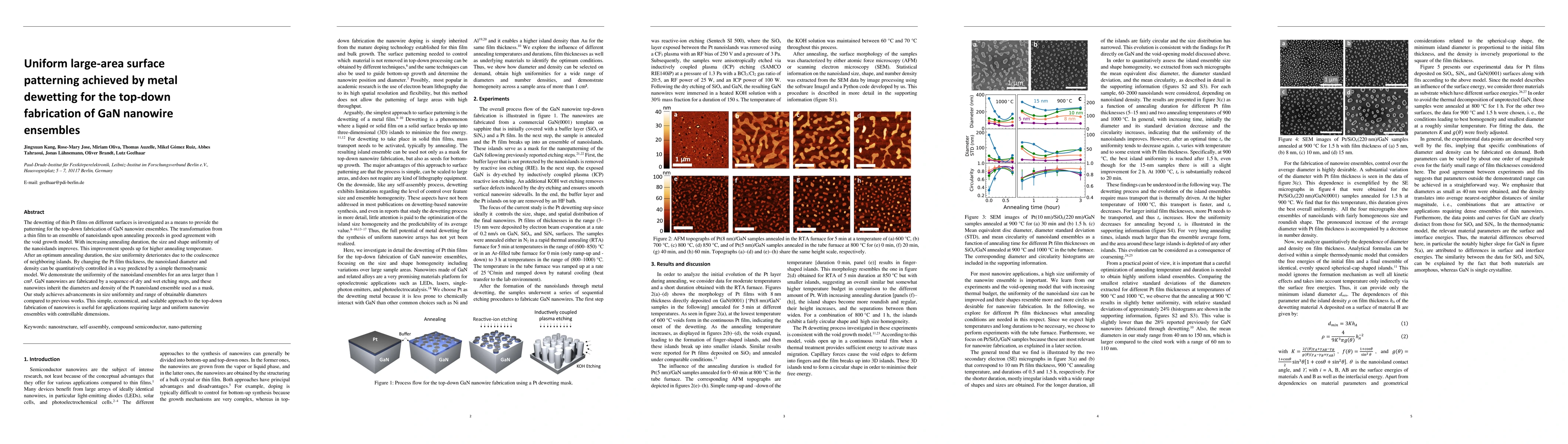
The dewetting of thin Pt films on different surfaces is investigated as a means to provide the patterning for the top-down fabrication of GaN nanowire ensembles. The transformation from a thin film ...
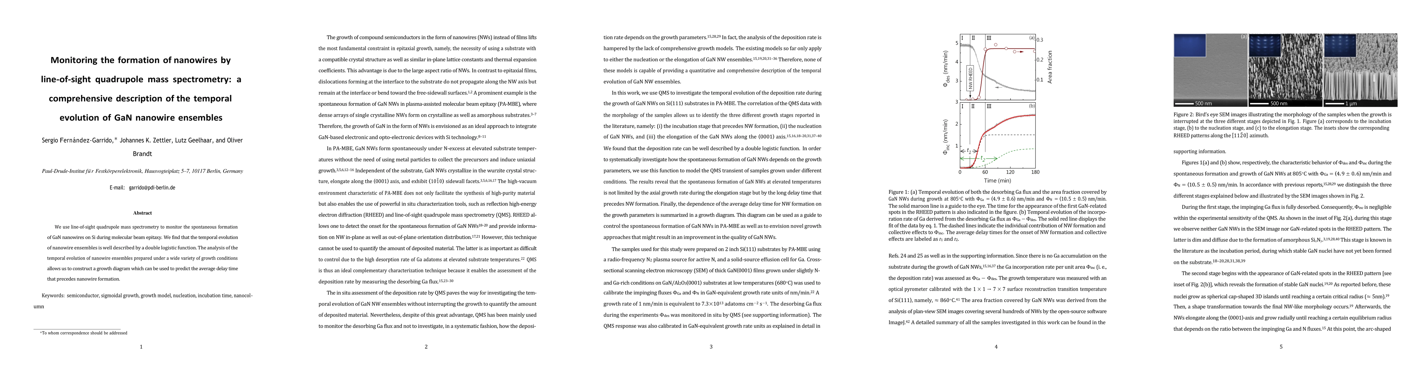
We use line-of-sight quadrupole mass spectrometry to monitor the spontaneous formation of GaN nanowires on Si during molecular beam epitaxy. We find that the temporal evolution of nanowire ensembles...
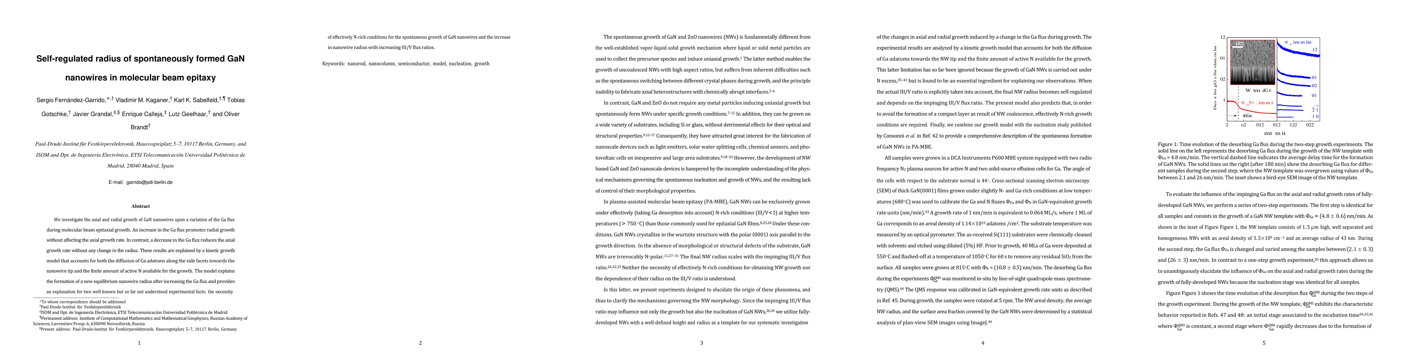
We investigate the axial and radial growth of GaN nanowires upon a variation of the Ga flux during molecular beam epitaxial growth. An increase in the Ga flux promotes radial growth without affectin...
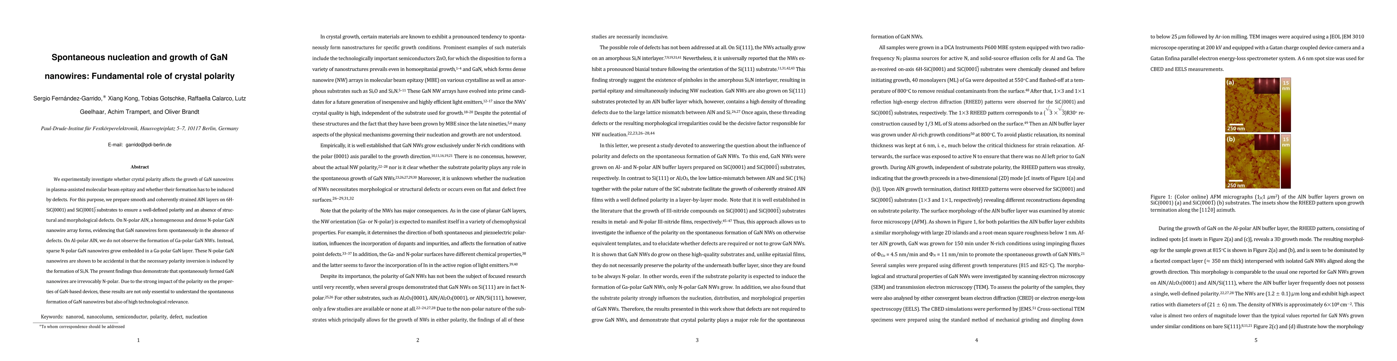
We experimentally investigate whether crystal polarity affects the growth of GaN nanowires in plasma-assisted molecular beam epitaxy and whether their formation has to be induced by defects. For thi...
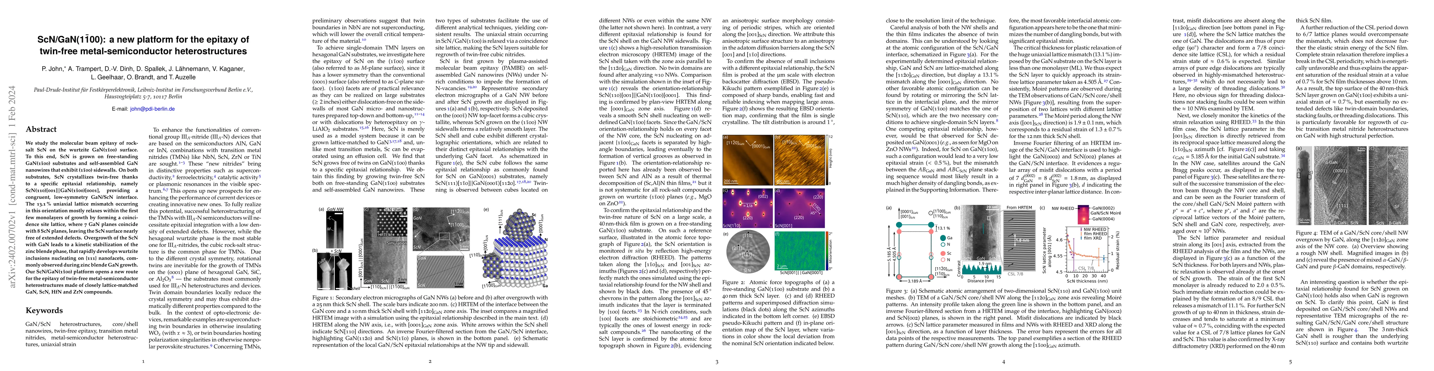
We study the molecular beam epitaxy of rock-salt ScN on the wurtzite GaN($1\bar{1}00$) surface. To this end, ScN is grown on free-standing GaN($1\bar{1}00$) substrates and self-assembled GaN nanowir...
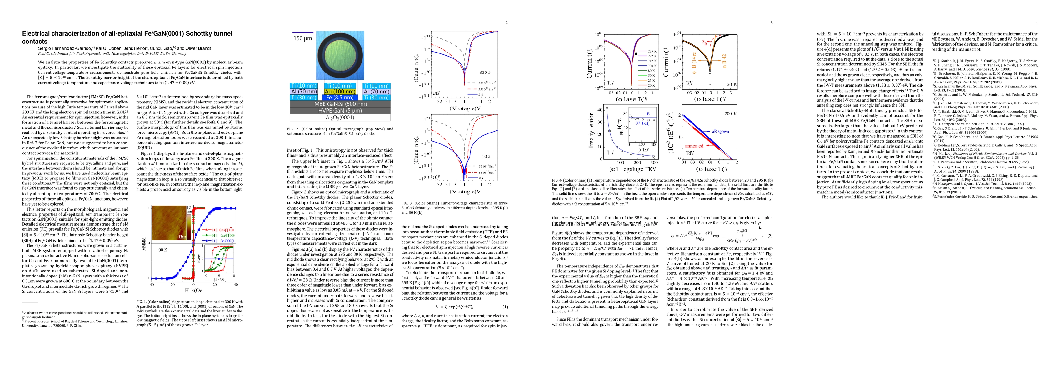
We analyze the properties of Fe Schottky contacts prepared in situ on n-type GaN(0001) by molecular beam epitaxy. In particular, we investigate the suitability of these epitaxial Fe layers for elect...
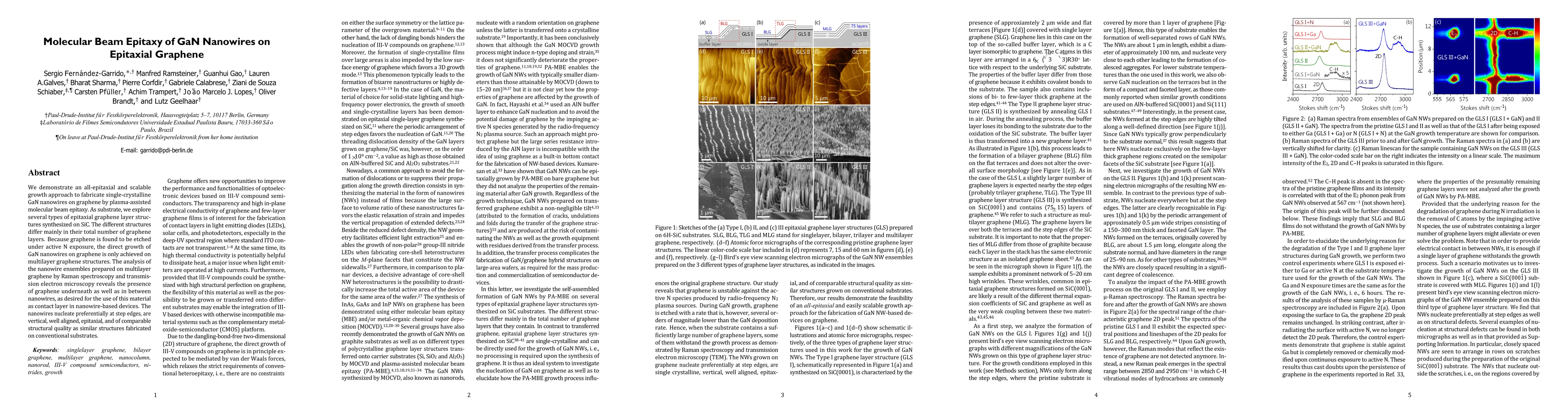
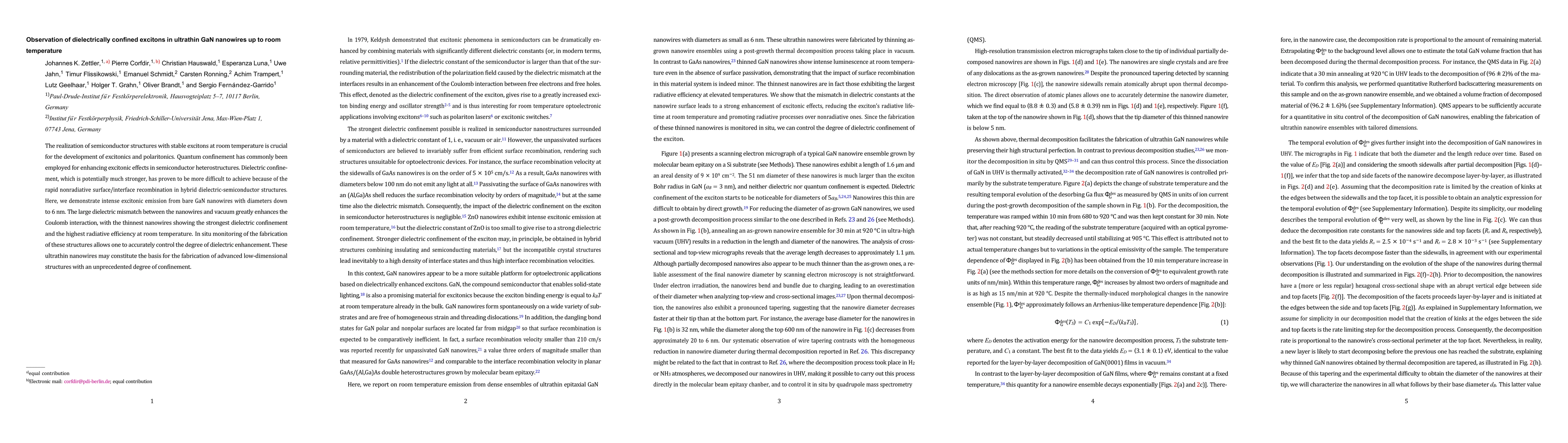
We demonstrate an all-epitaxial and scalable growth approach to fabricate single-crystalline GaN nanowires on graphene by plasma-assisted molecular beam epitaxy. As substrate, we explore several typ...
The realization of semiconductor structures with stable excitons at room temperature is crucial for the development of excitonics and polaritonics. Quantum confinement has commonly been employed for...
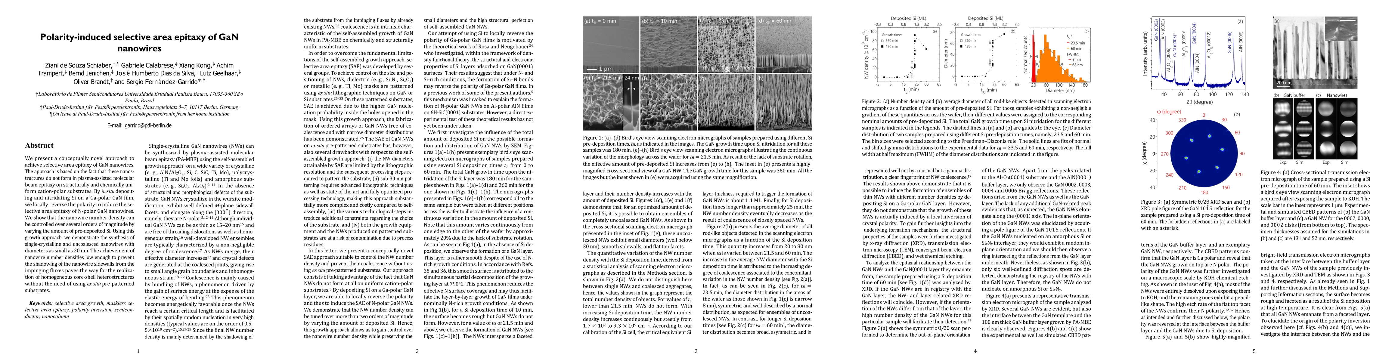
We present a conceptually novel approach to achieve selective area epitaxy of GaN nanowires. The approach is based on the fact that these nanostructures do not form in plasma-assisted molecular beam...
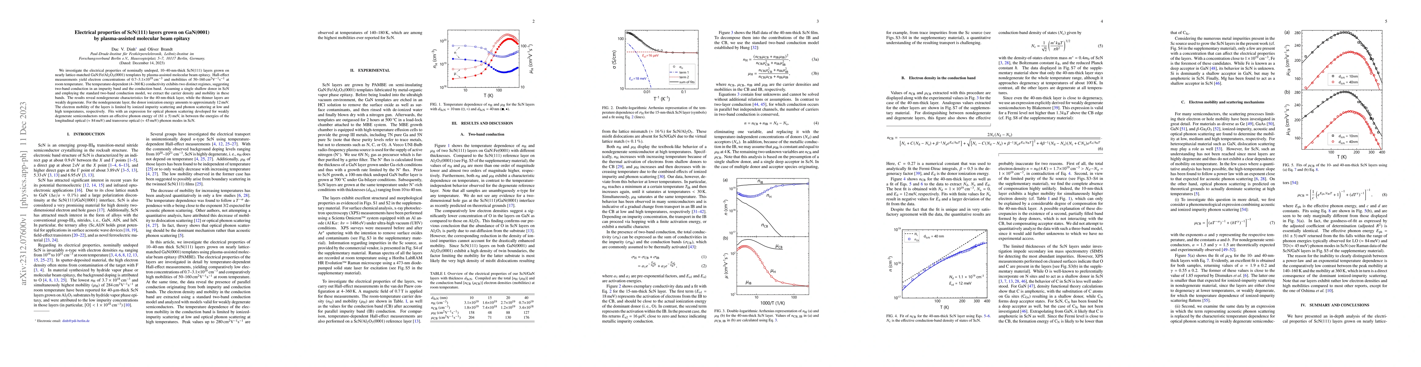
We investigate the electrical properties of nominally undoped, 10-40-nm-thick ScN(111) layers grown on nearly lattice-matched GaN:Fe/Al$_2$O$_3$(0001) templates by plasma-assisted molecular beam epi...
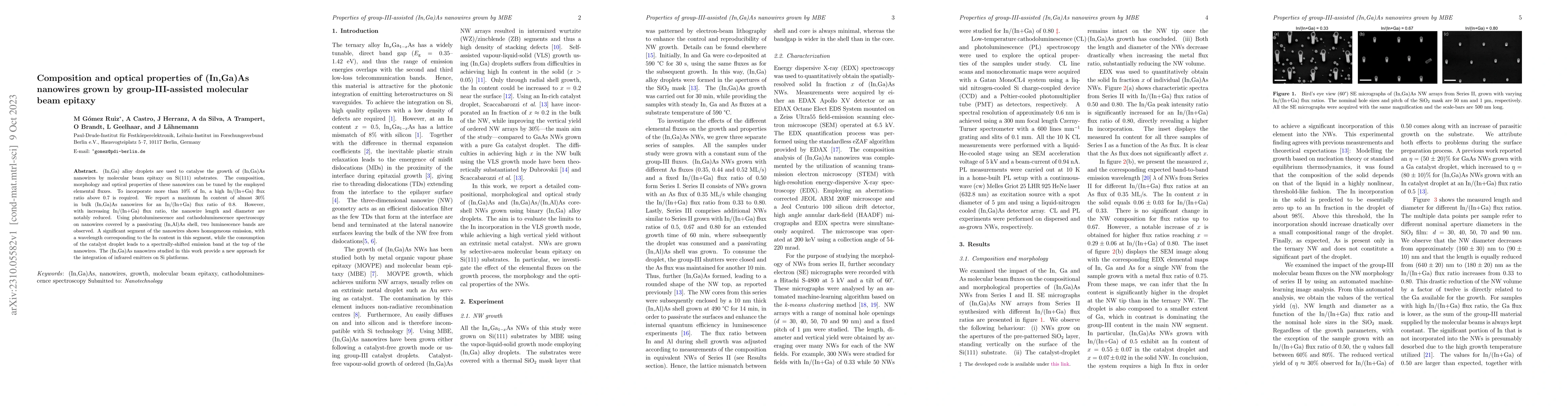
(In,Ga) alloy droplets are used to catalyse the growth of (In,Ga)As nanowires by molecular beam epitaxy on Si(111) substrates. The composition, morphology and optical properties of these nanowires c...
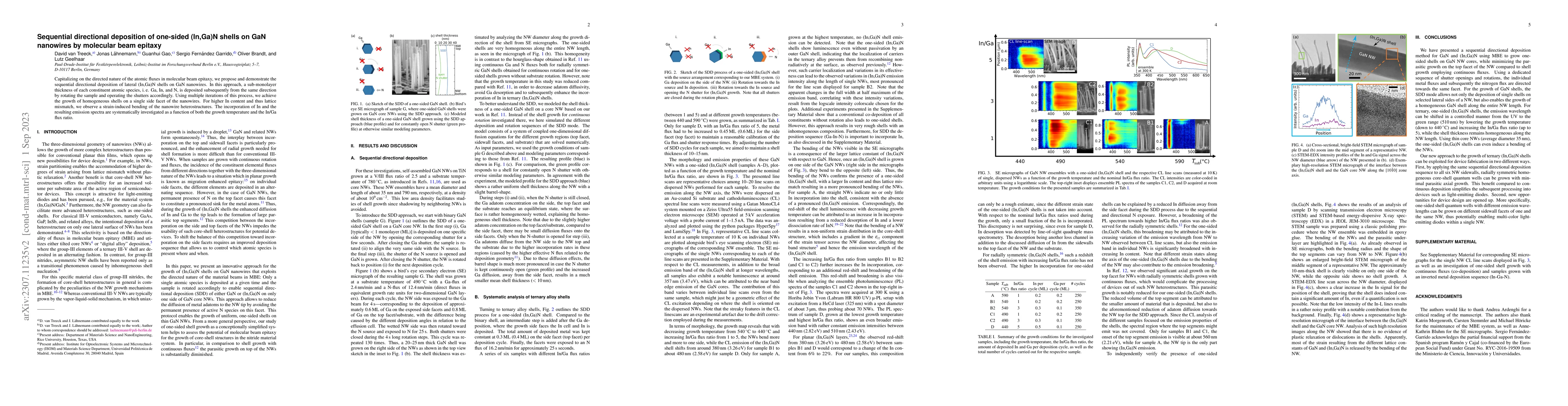
Capitalizing on the directed nature of the atomic fluxes in molecular beam epitaxy, we propose and demonstrate the sequential directional deposition of lateral (In,Ga)N shells on GaN nanowires. In t...
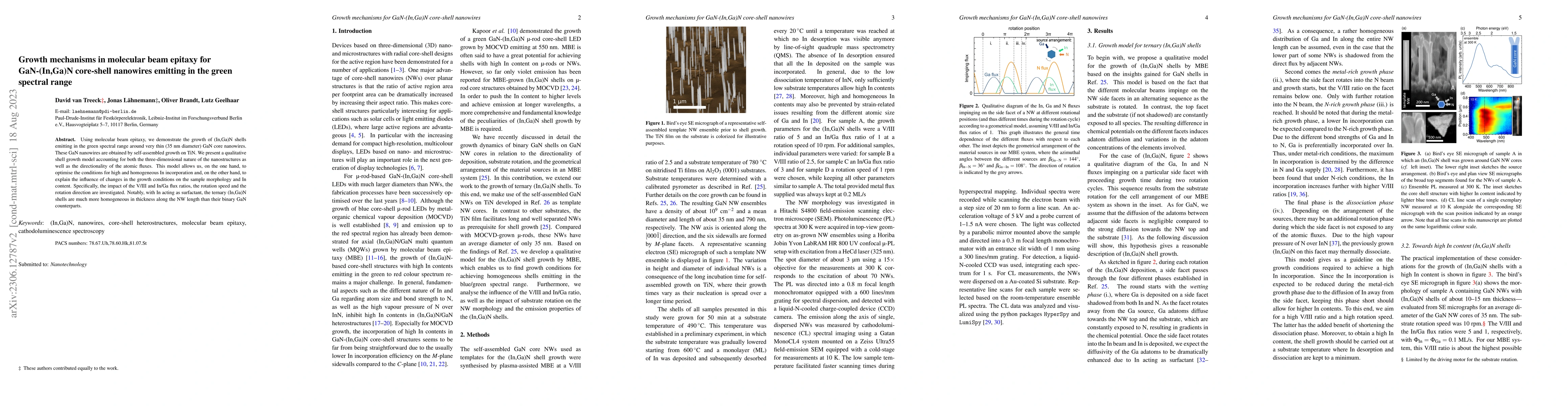
Using molecular beam epitaxy, we demonstrate the growth of (In,Ga)N shells emitting in the green spectral range around very thin (35 nm diameter) GaN core nanowires. These GaN nanowires are obtained...
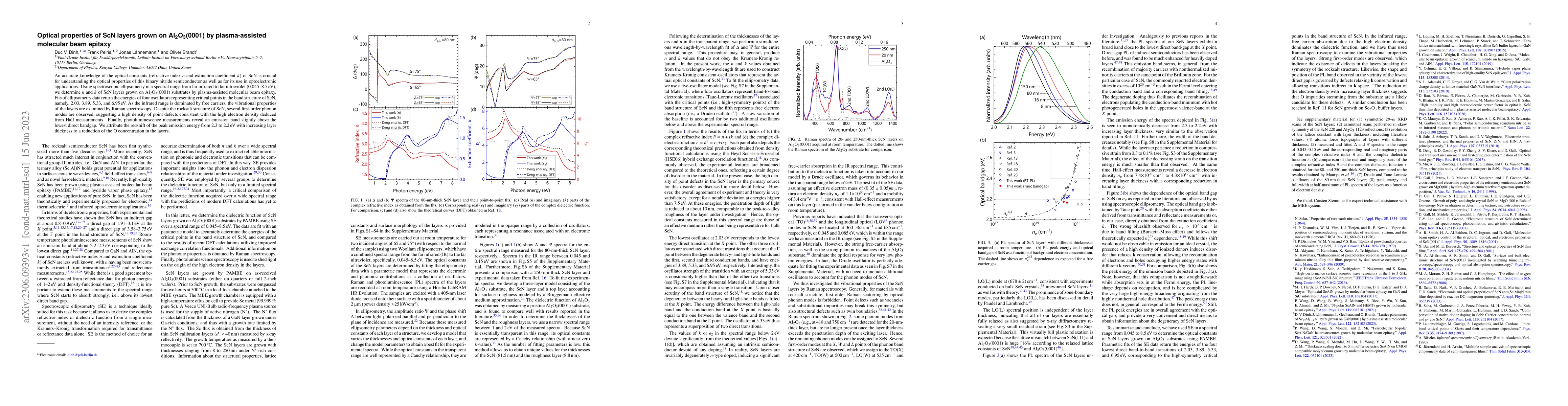
An accurate knowledge of the optical constants (refractive index $n$ and extinction coefficient $k$) of ScN is crucial for understanding the optical properties of this binary nitride semiconductor a...
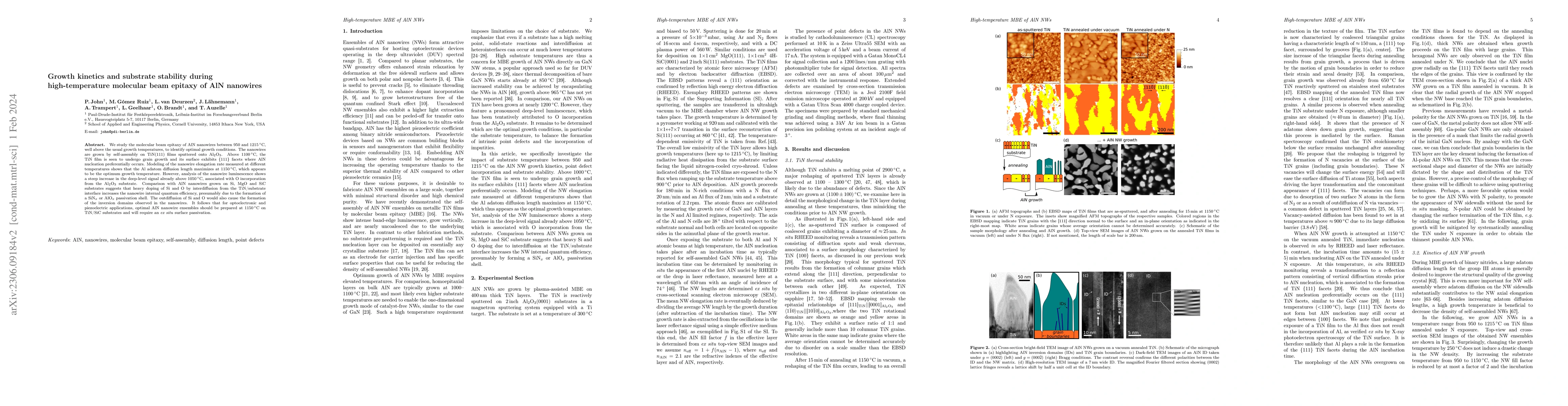
We study the molecular beam epitaxy of AlN nanowires between 950 and 1215 {\deg}C, well above the usual growth temperatures, to identify optimal growth conditions. The nanowires are grown by self-as...
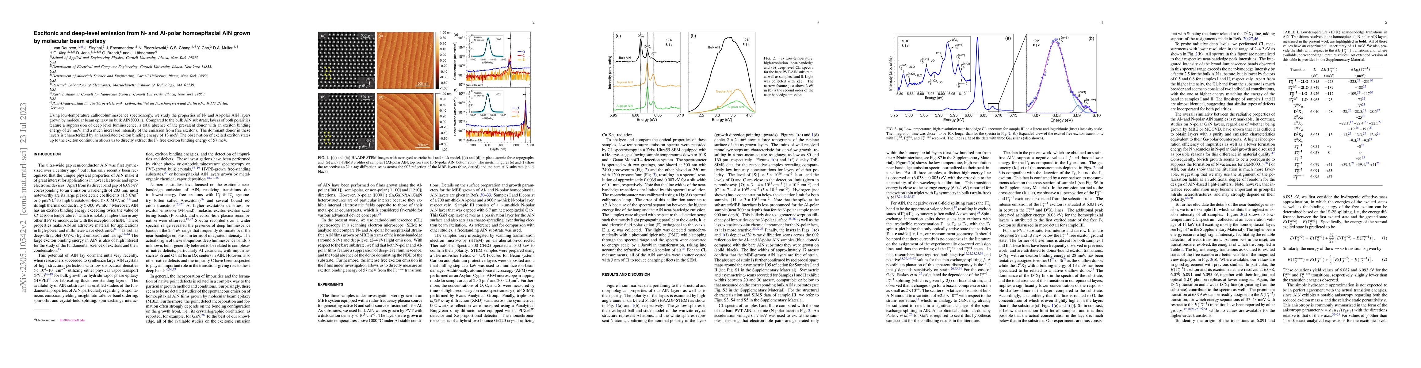
Using low-temperature cathodoluminescence spectroscopy, we study the properties of N- and Al-polar AlN layers grown by molecular beam epitaxy on bulk AlN{0001}. Compared to the bulk AlN substrate, l...
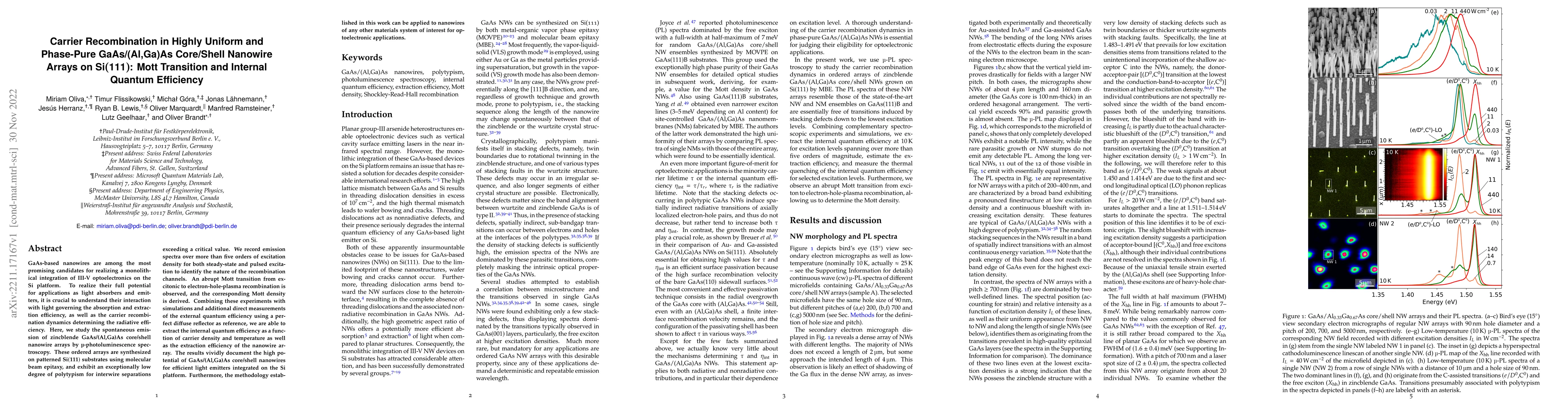
GaAs-based nanowires are among the most promising candidates for realizing a monolithical integration of III-V optoelectronics on the Si platform. To realize their full potential for applications as...
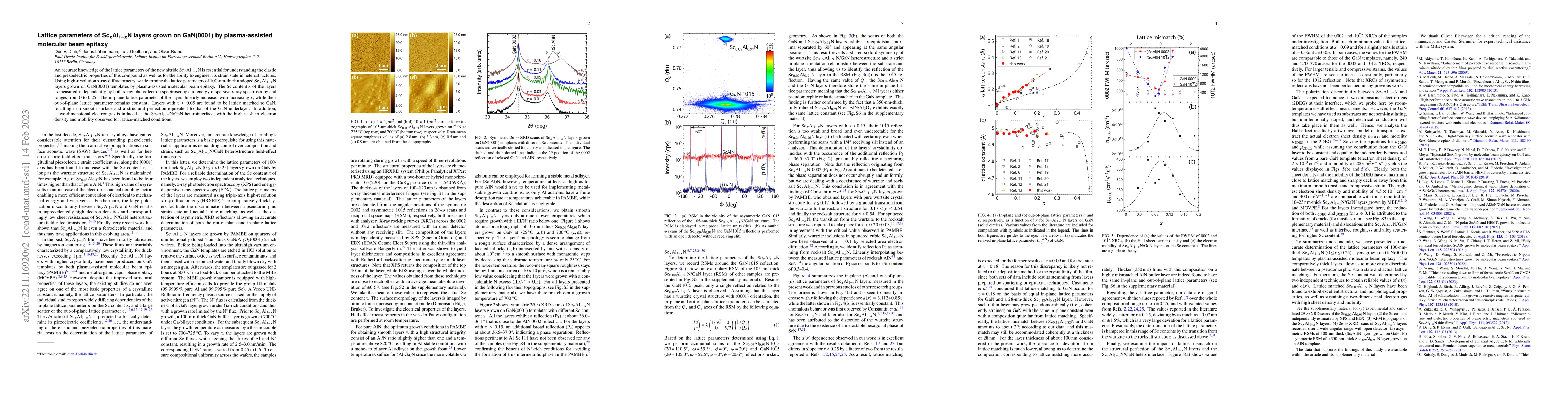
An accurate knowledge of the lattice parameters of the new nitride Sc$_\textit{x}$Al$_\textit{1-x}$N is essential for understanding the elastic and piezoelectric properties of this compound as well ...
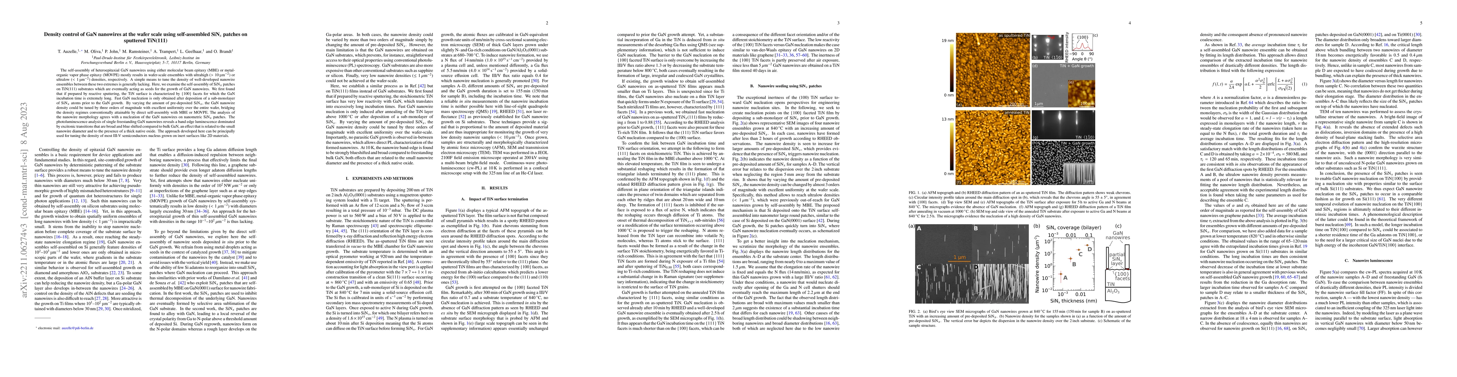
The self-assembly of heteroepitaxial GaN nanowires using either molecular beam epitaxy (MBE) or metal-organic vapor phase epitaxy (MOVPE) mostly results in wafer-scale ensembles with ultrahigh ($>10...
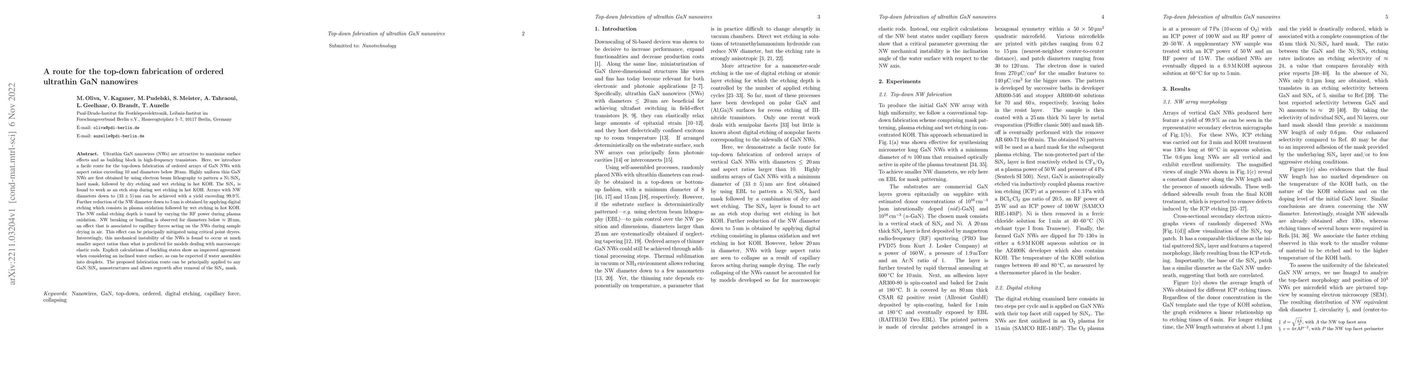
Ultrathin GaN nanowires (NWs) are attractive to maximize surface effects and as building block in high-frequency transistors. Here, we introduce a facile route for the top-down fabrication of ordere...
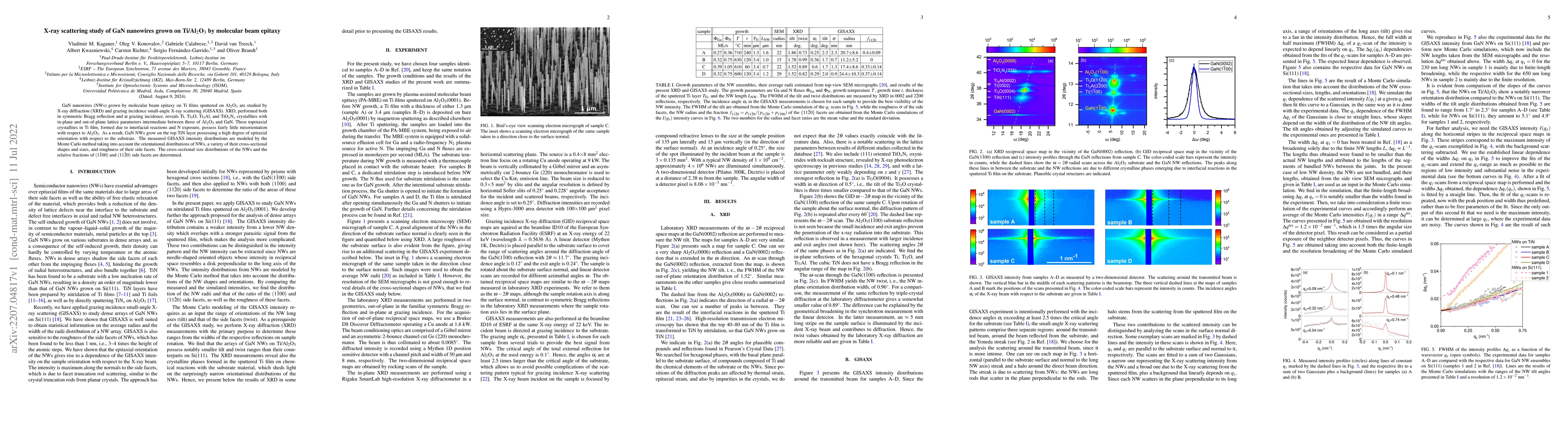
GaN nanowires (NWs) grown by molecular beam epitaxy on Ti films sputtered on Al$_{2}$O$_{3}$ are studied by X-ray diffraction (XRD) and grazing incidence small-angle X-ray scattering (GISAXS). XRD, ...
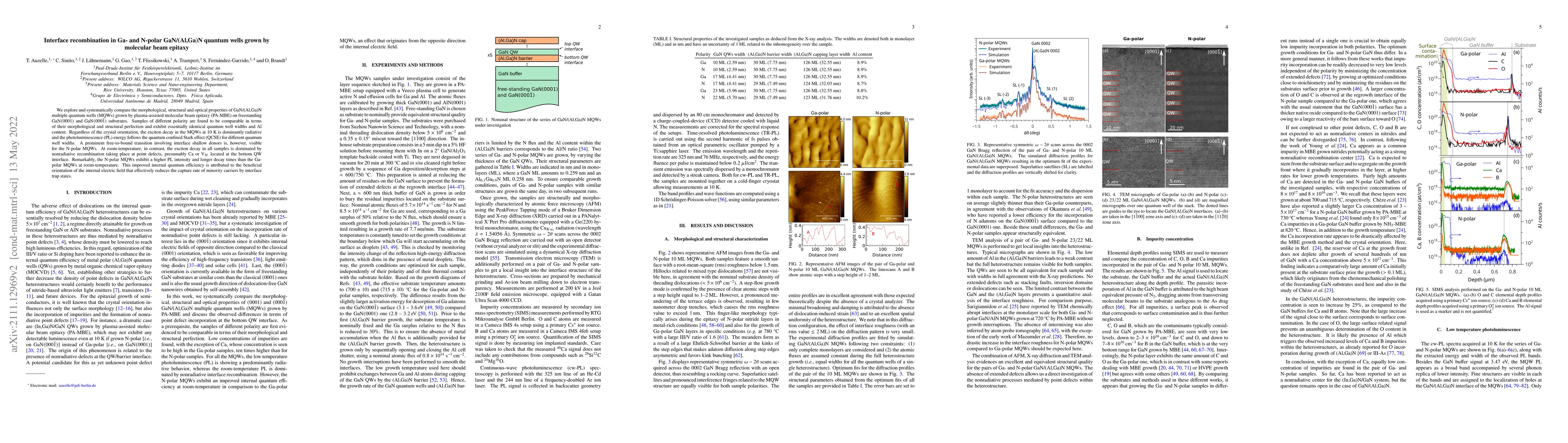
We explore and systematically compare the morphological, structural and optical properties of GaN/(Al,Ga)N multiple quantum wells (MQWs) grown by plasma-assisted molecular beam epitaxy (PA-MBE) on f...
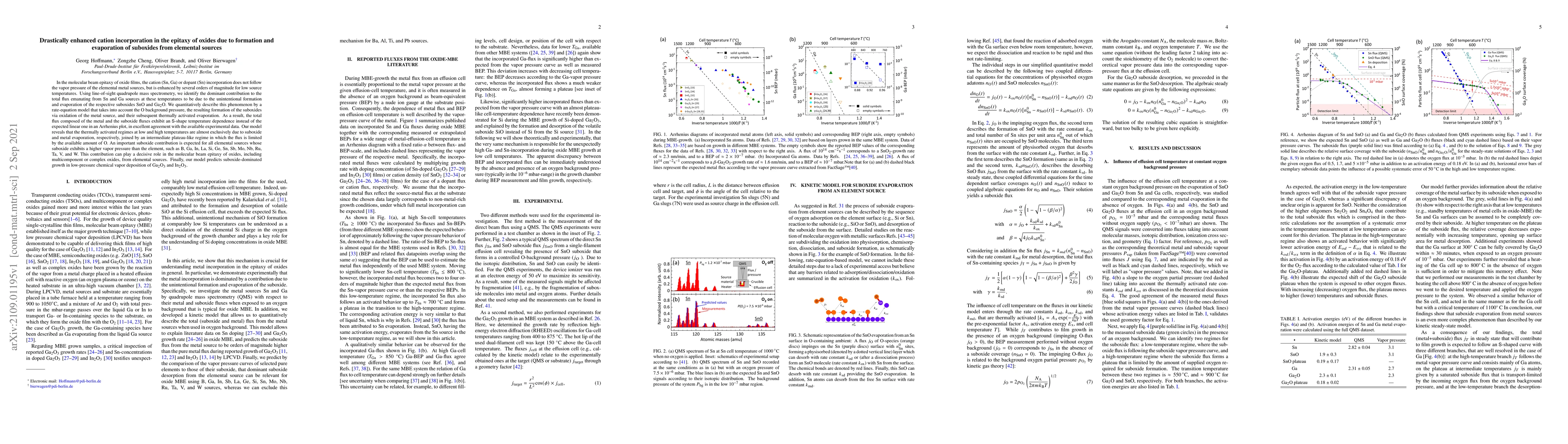
In the molecular beam epitaxy of oxide films, the cation (Sn, Ga) or dopant (Sn) incorporation does not follow the vapor pressure of the elemental metal sources, but is enhanced by several orders of...
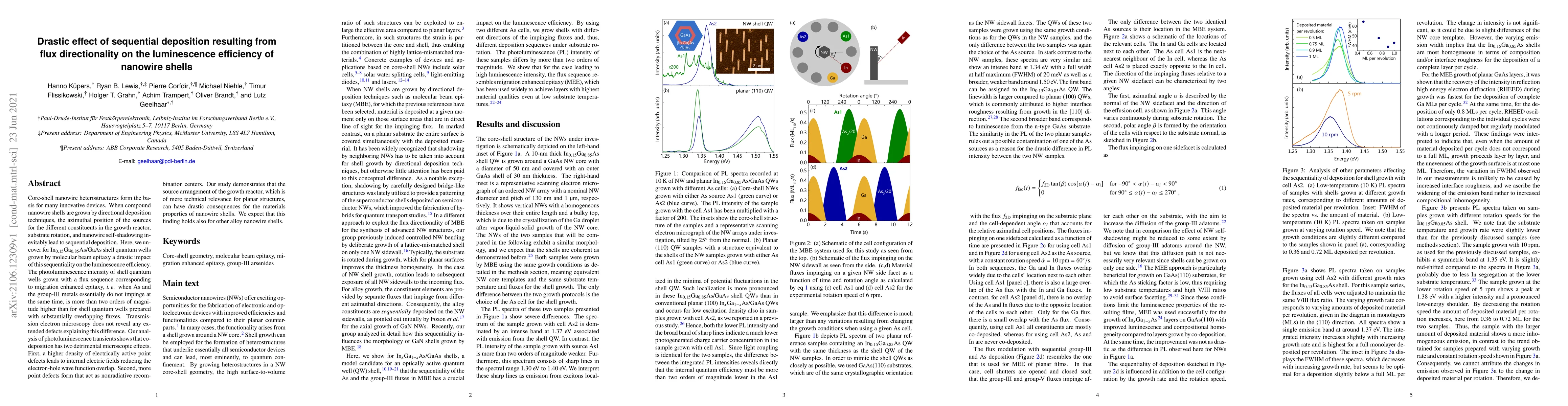
Core-shell nanowire heterostructures form the basis for many innovative devices. When compound nanowire shells are grown by directional deposition techniques, the azimuthal position of the sources f...
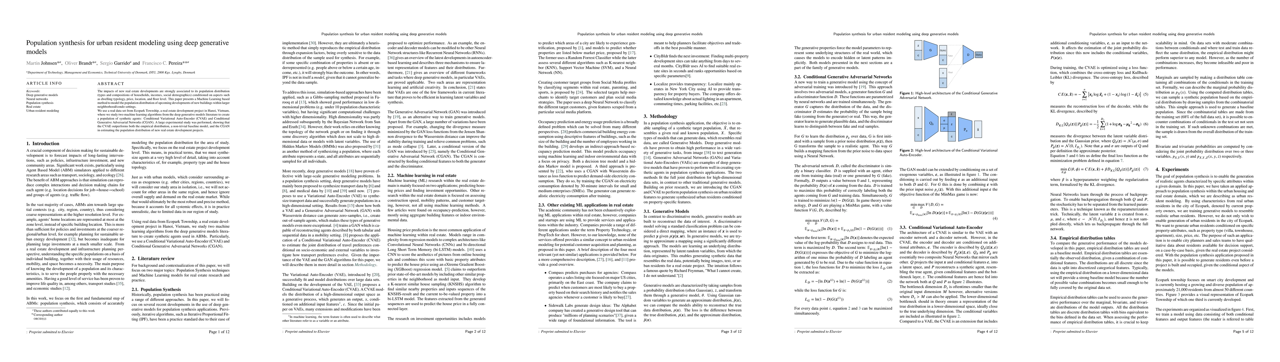
The impacts of new real estate developments are strongly associated to its population distribution (types and compositions of households, incomes, social demographics) conditioned on aspects such as...
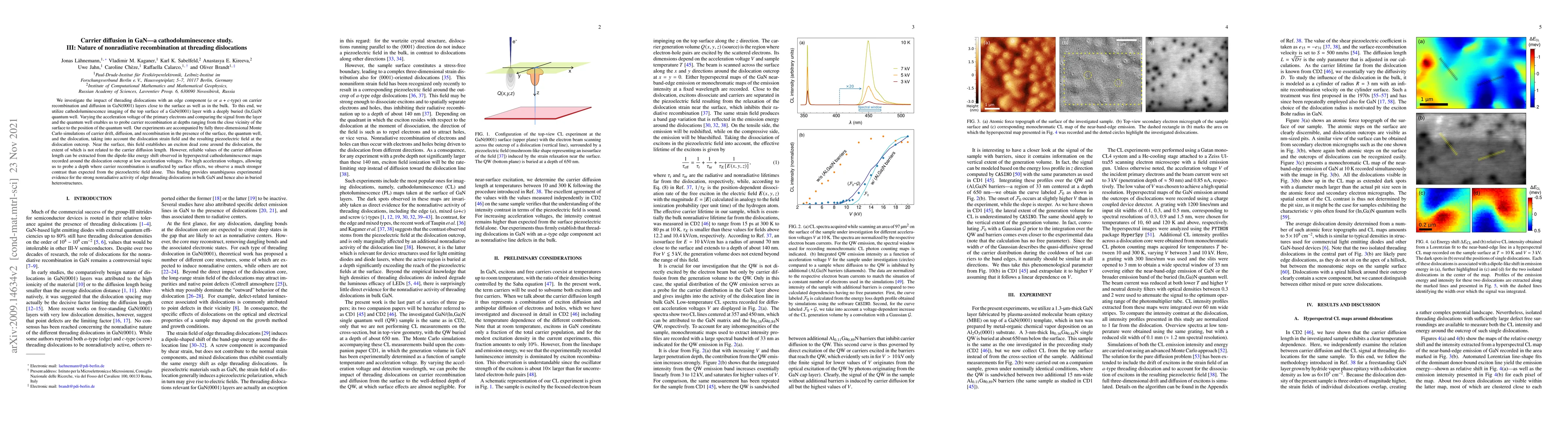
We investigate the impact of threading dislocations with an edge component (a or a+c-type) on carrier recombination and diffusion in GaN(0001) layers close to the surface as well as in the bulk. To ...
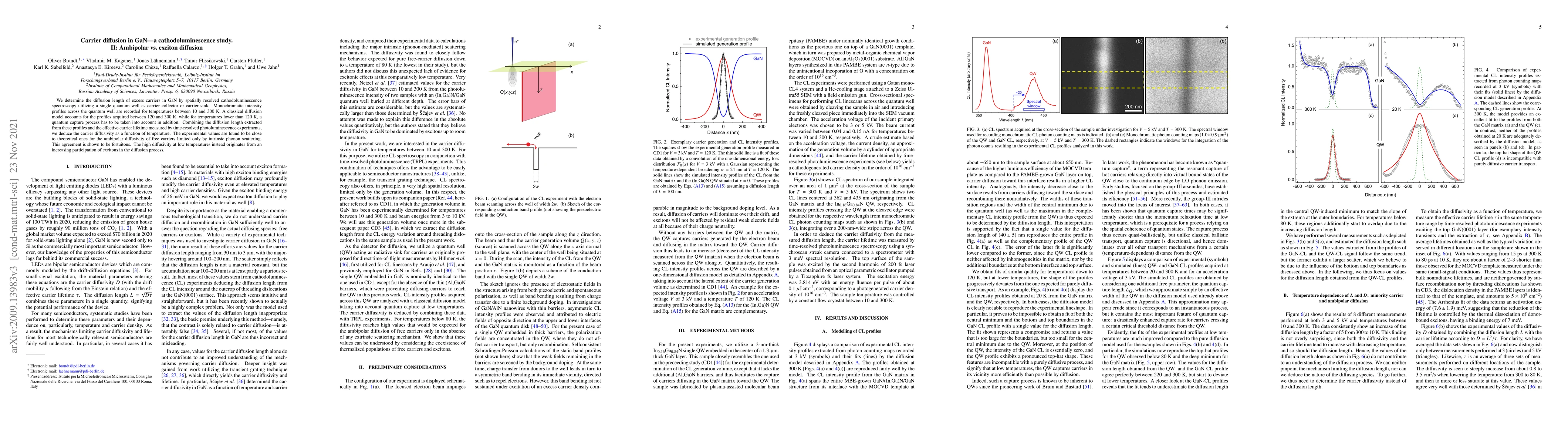
We determine the diffusion length of excess carriers in GaN by spatially resolved cathodoluminescence spectroscopy utilizing a single quantum well as carrier collector or carrier sink. Monochromatic...
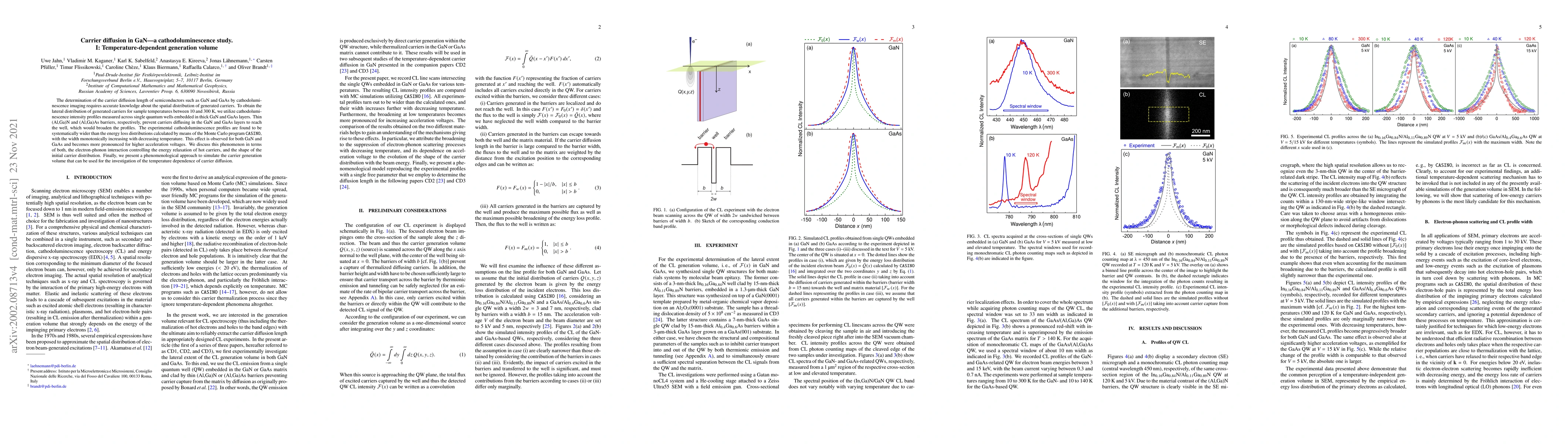
The determination of the carrier diffusion length of semiconductors such as GaN and GaAs by cathodoluminescence imaging requires accurate knowledge about the spatial distribution of generated carrie...
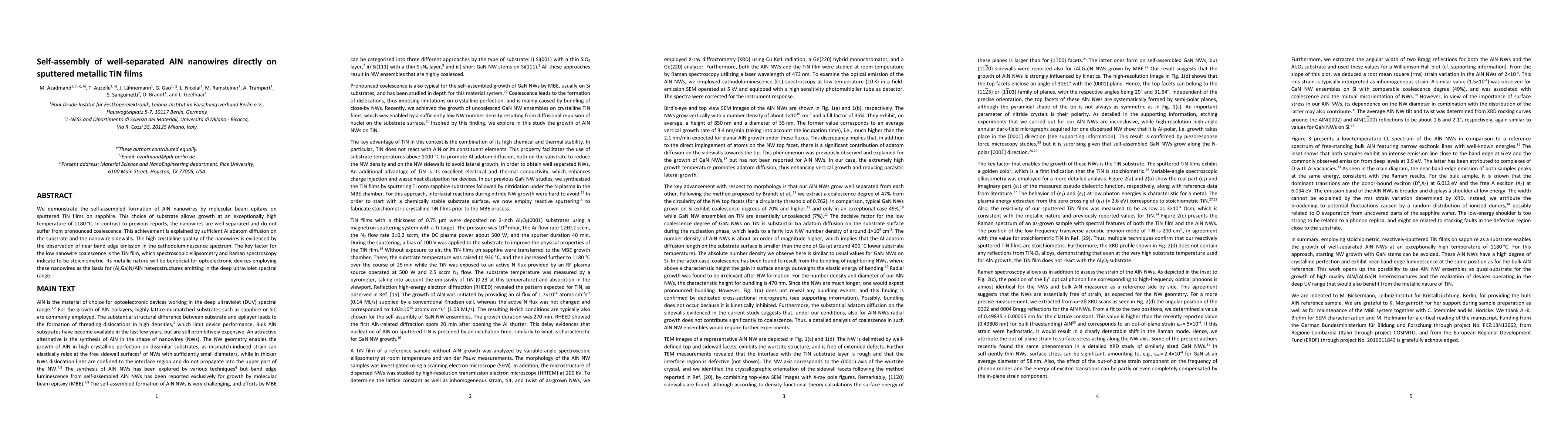
We demonstrate the self-assembled formation of AlN nanowires by molecular beam epitaxy on sputtered TiN films on sapphire. This choice of substrate allows growth at an exceptionally high temperature...
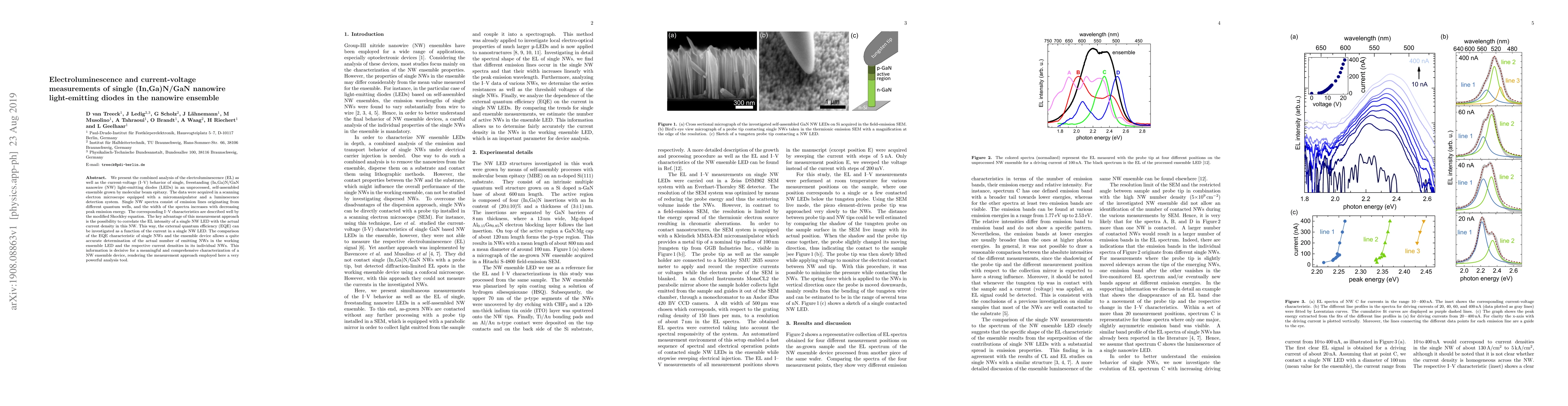
We present the combined analysis of the electroluminescence (EL) as well as the current-voltage (I-V) behavior of single, freestanding (In,Ga)N/GaN nanowire (NW) light-emitting diodes (LEDs) in an u...
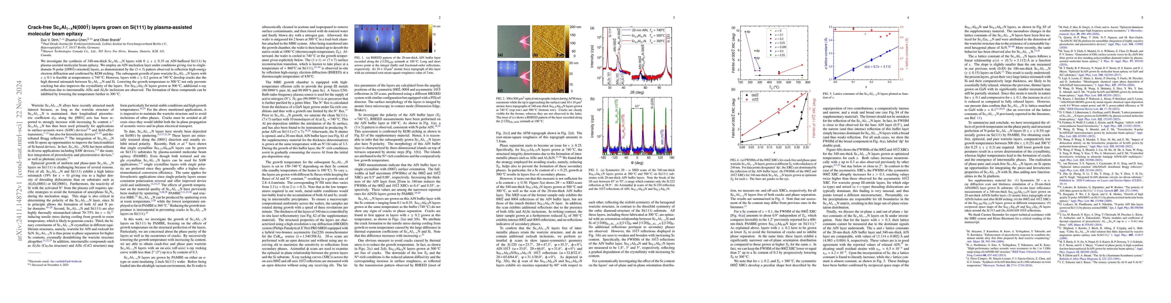
We investigate the synthesis of 340-nm-thick Sc$_x$Al$_{1-x}$N layers with $0 \leq x \leq 0.35$ on AlN-buffered Si(111) by plasma-assisted molecular beam epitaxy. We employ an AlN nucleation layer und...
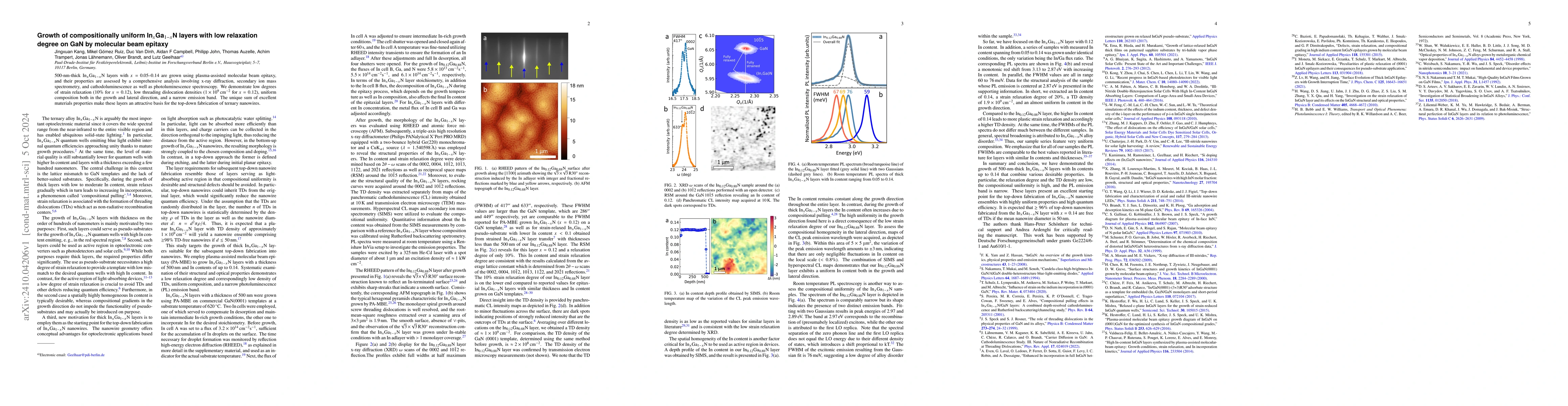
500-nm-thick $\mathrm{In}_{x}\mathrm{Ga}_{1-x}\mathrm{N}$ layers with $x=$ 0.05-0.14 are grown using plasma-assisted molecular beam epitaxy, and their properties are assessed by a comprehensive analys...
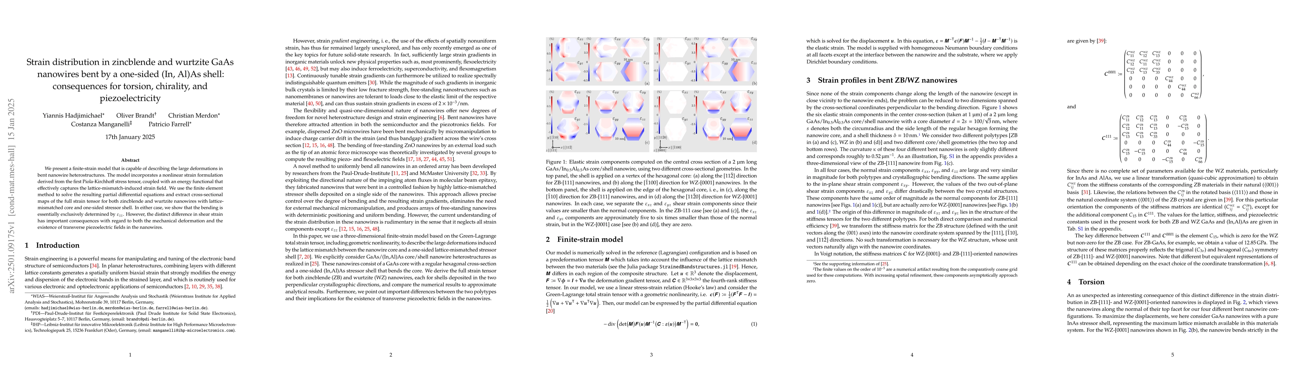
We present a finite-strain model that is capable of describing the large deformations in bent nanowire heterostructures. The model incorporates a nonlinear strain formulation derived from the first Pi...
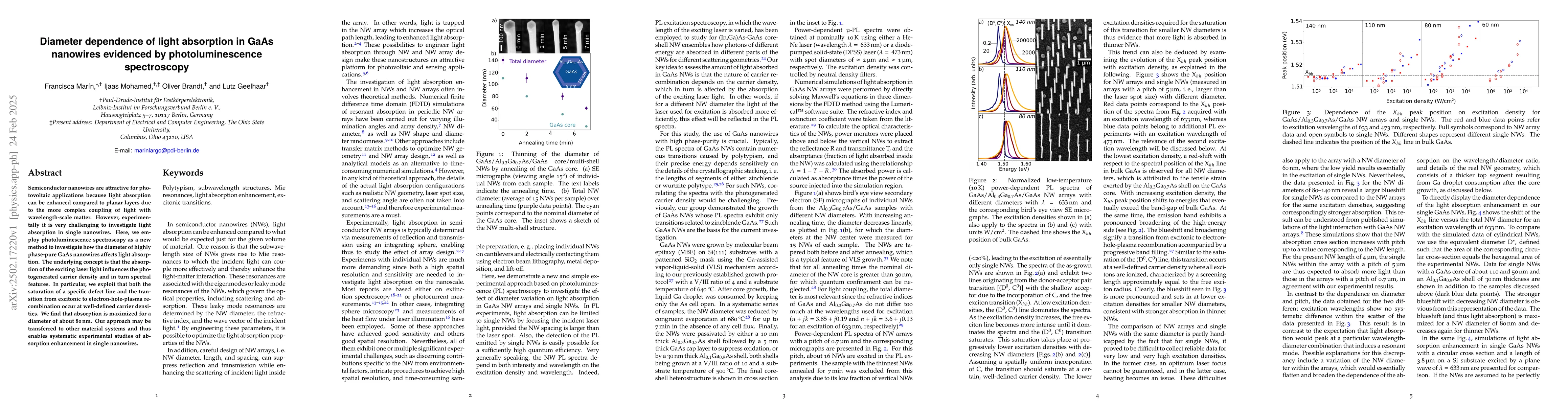
Semiconductor nanowires are attractive for photovoltaic applications because light absorption can be enhanced compared to planar layers due to the more complex coupling of light with wavelength-scale ...
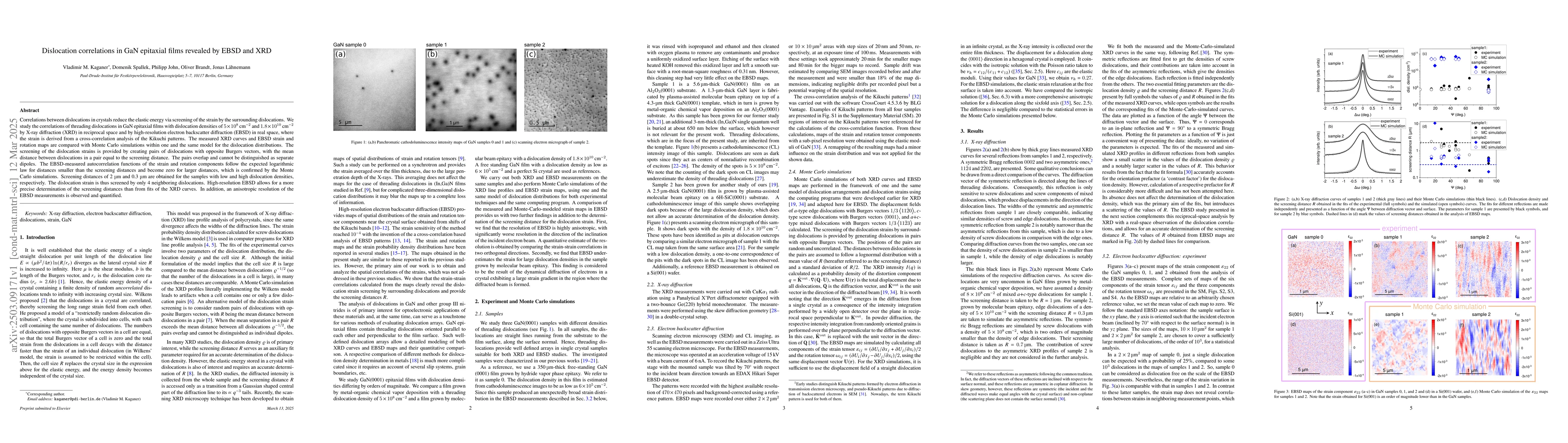
Correlations between dislocations in crystals reduce the elastic energy via screening of the strain by the surrounding dislocations. We study the correlations of threading dislocations in GaN epitaxia...
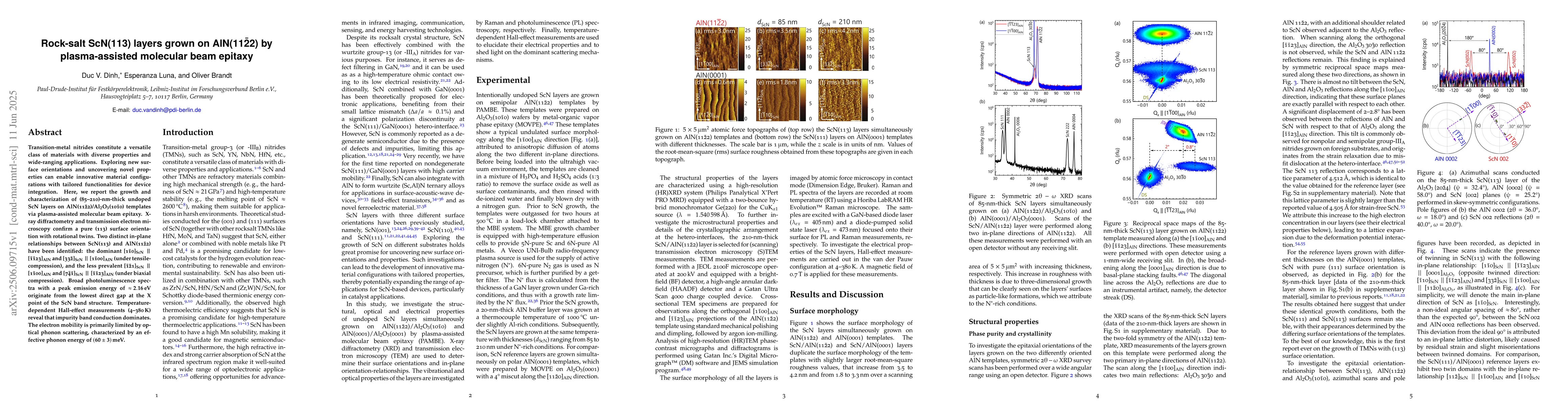
Transition-metal nitrides constitute a versatile class of materials with diverse properties and wide-ranging applications. Exploring new surface orientations and uncovering novel properties can enable...
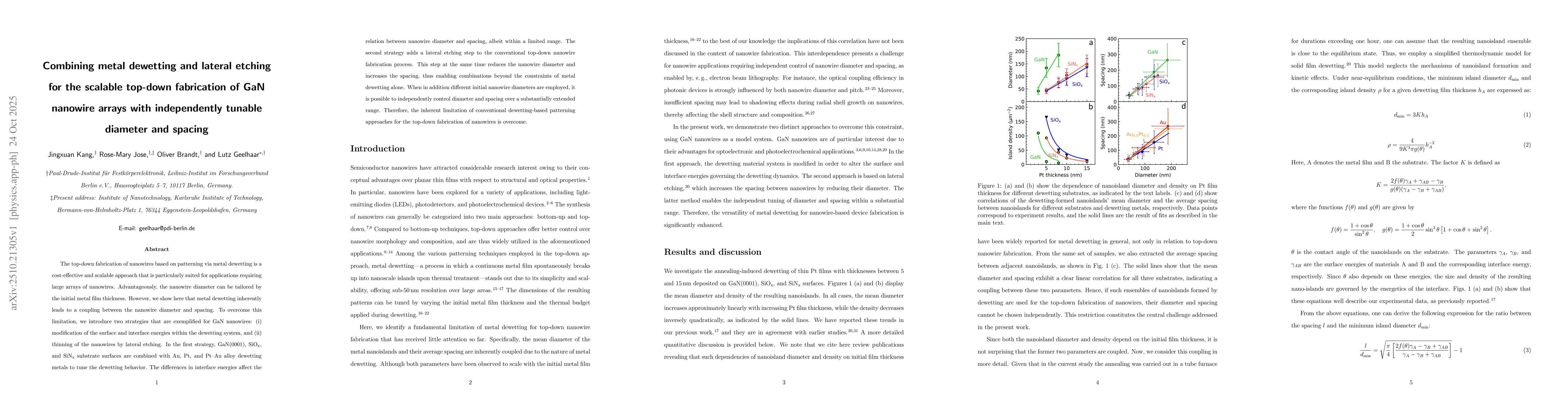
The top-down fabrication of nanowires based on patterning via metal dewetting is a cost-effective and scalable approach that is particularly suited for applications requiring large arrays of nanowires...
We present a comprehensive optical characterization of 200-nm-thick CrN(111) films grown simultaneously on Al$_2$O$_3$(0001) and AlN/Al$_2$O$_3$(0001) using plasma-assisted molecular beam epitaxy. Spe...
The transport properties and electrical bandgap of nominally undoped ~75-nm-thick CrN layers simultaneously grown on AlN(0001) and AlN(11\bar{2}2) templates using plasma-assisted molecular beam epitax...
We fabricate (In,Ga)N pseudo-substrates with a total thickness of ~1 um grown on GaN templates using plasma-assisted molecular beam epitaxy. In a three-step process, we change growth conditions from N...
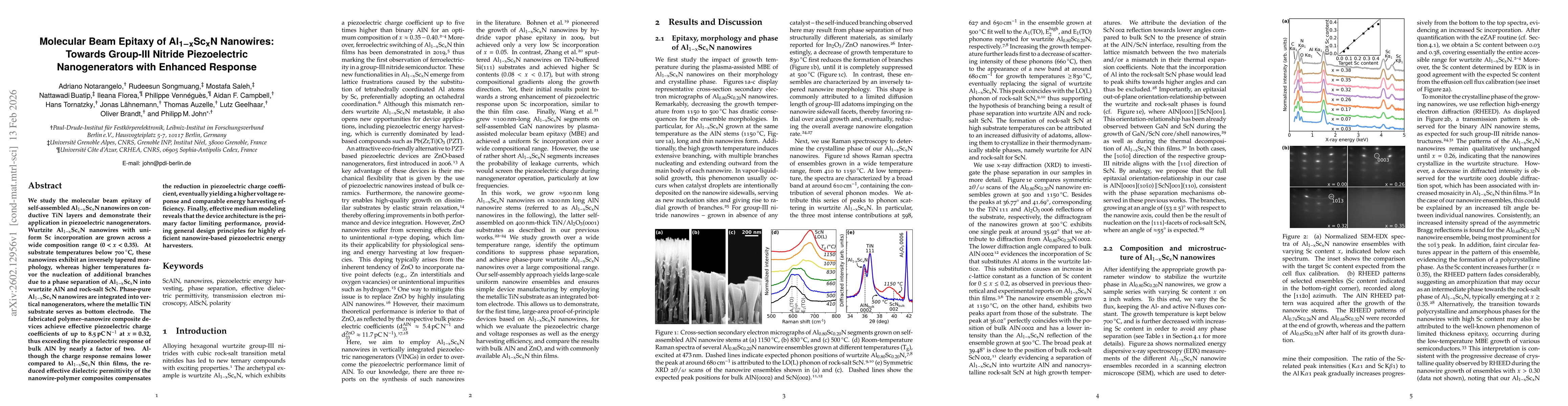
We study the molecular beam epitaxy of self-assembled Al$\mathrm{_{1-x}}$Sc$\mathrm{_{x}}$N nanowires on conductive TiN layers and demonstrate their application in piezoelectric nanogenerators. Wurtzi...
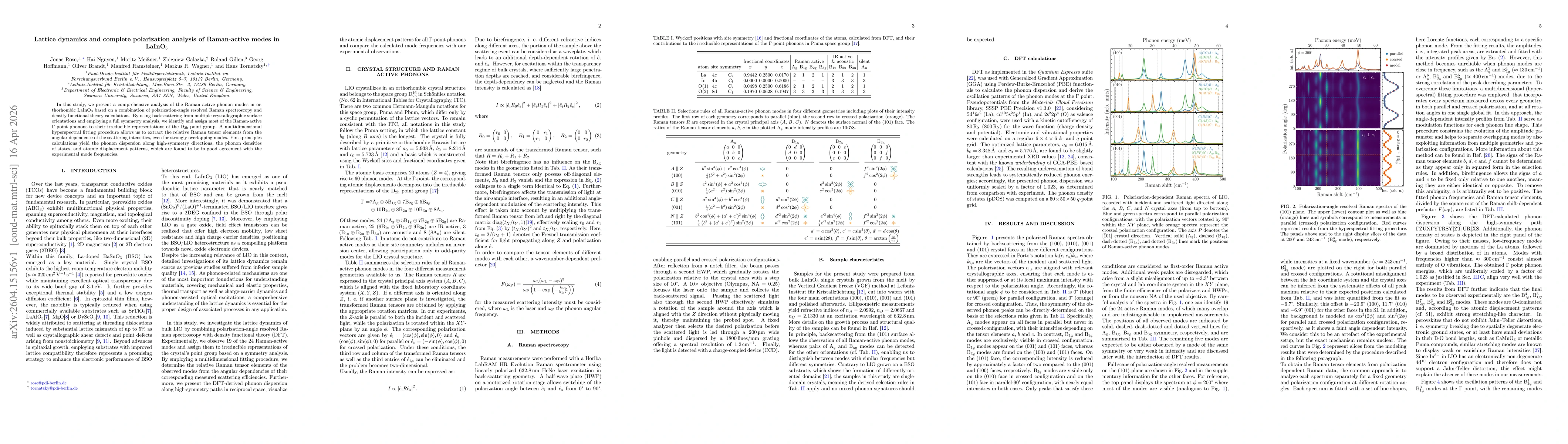
In this study, we present a comprehensive analysis of the Raman active phonon modes in orthorhombic LaInO$_3$ based on a combination of polarization-angle resolved Raman spectroscopy and density funct...
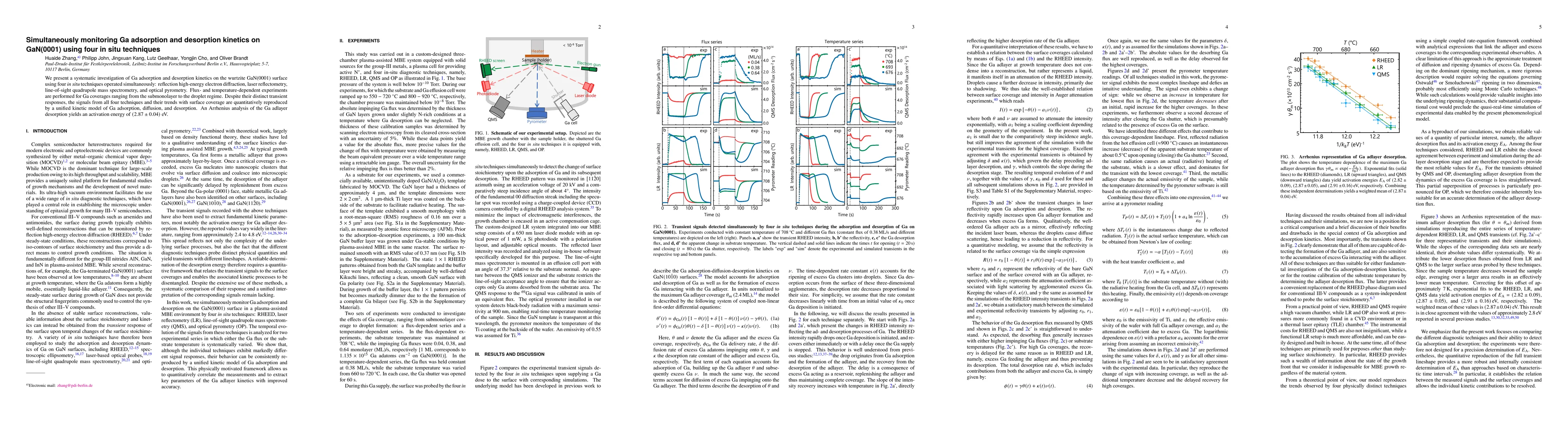
We present a systematic investigation of Ga adsorption and desorption kinetics on the wurtzite GaN(0001) surface using four in situ techniques operated simultaneously: reflection high-energy electron ...