ArxivLens
S
Researcher

Sergio Fernández-Garrido

12 papers on arXiv

12 arXiv Papers
5 Total Publications
Profile

Academic Profile

Name S. F. Garrido
Total Papers 5
Scholar Profile View on Semantic Scholar
Metrics

Statistics

12 arXiv Papers
5 Total Publications
Publications

Papers on arXiv

Thumbnail for Optomechanical cavities based on epitaxial GaP on nominally
  (001)-oriented Si
arXiv
Optomechanical cavities based on epitaxial GaP on nominally (001)-oriented Si

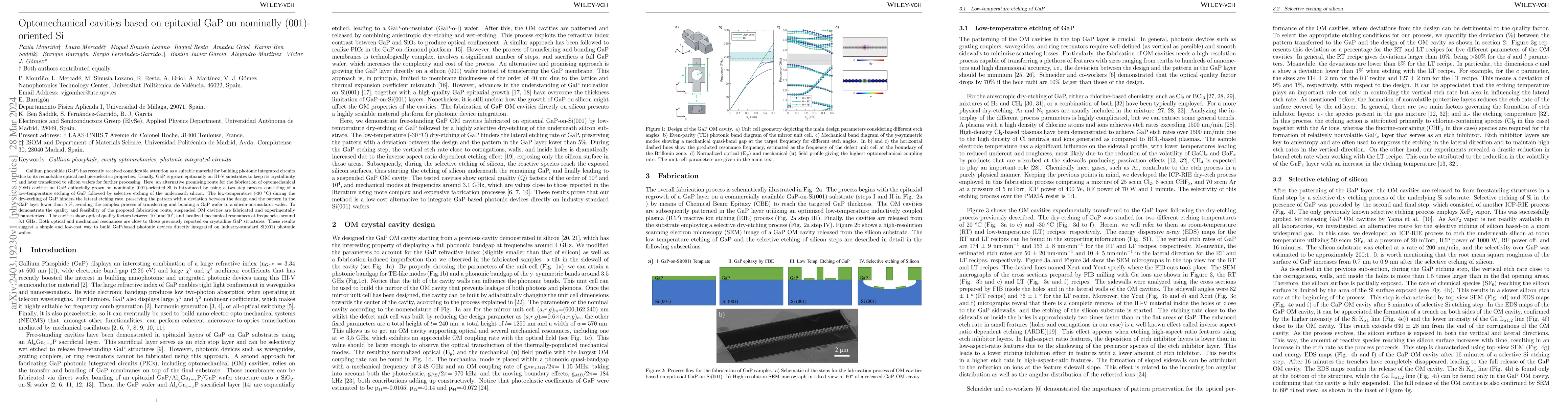
Gallium phosphide (GaP) has recently received considerable attention as a suitable material for building photonic integrated circuits due to its remarkable optical and piezoelectric properties. Usua...

Thumbnail for Monitoring the formation of nanowires by line-of-sight quadrupole mass
  spectrometry: a comprehensive description of the temporal evolution of GaN
  nanowire ensembles
arXiv
Monitoring the formation of nanowires by line-of-sight quadrupole mass spectrometry: a comprehensive description of the temporal evolution of GaN nanowire ensembles

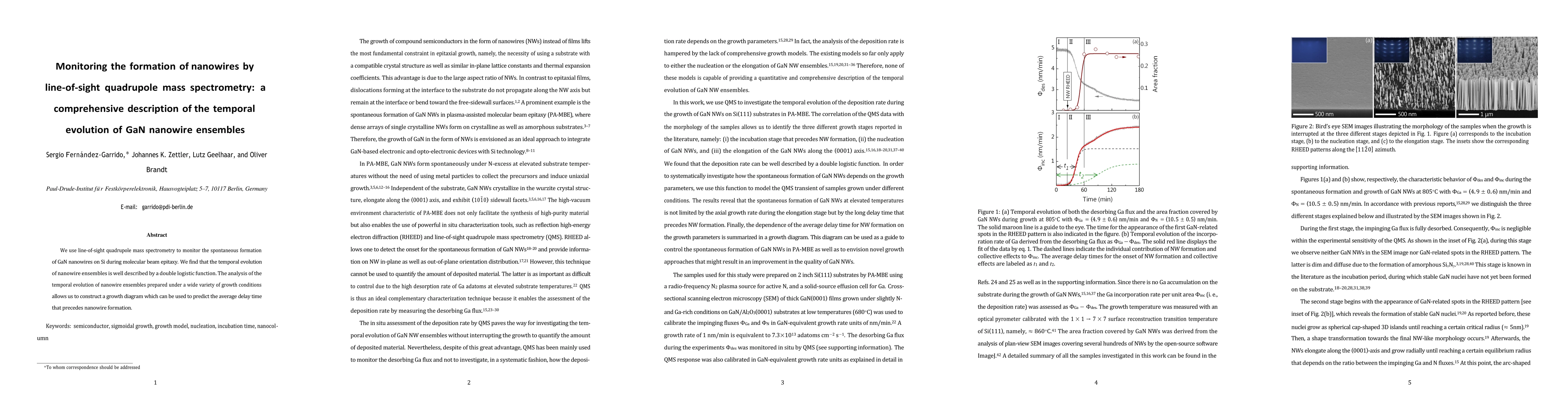
We use line-of-sight quadrupole mass spectrometry to monitor the spontaneous formation of GaN nanowires on Si during molecular beam epitaxy. We find that the temporal evolution of nanowire ensembles...

Thumbnail for Self-regulated radius of spontaneously formed GaN nanowires in molecular
  beam epitaxy
arXiv
Self-regulated radius of spontaneously formed GaN nanowires in molecular beam epitaxy

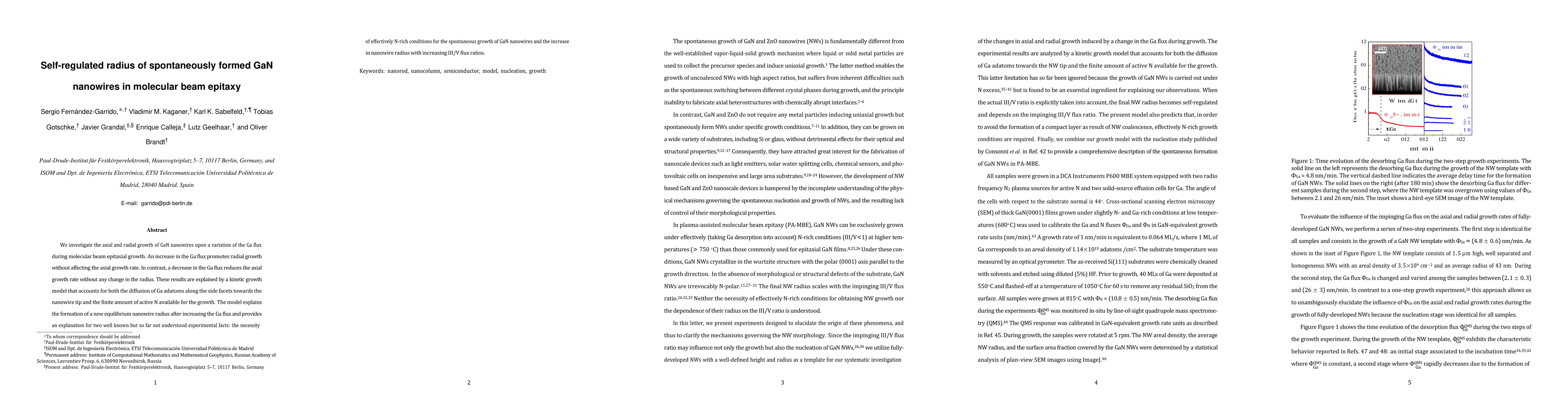
We investigate the axial and radial growth of GaN nanowires upon a variation of the Ga flux during molecular beam epitaxial growth. An increase in the Ga flux promotes radial growth without affectin...

Thumbnail for Spontaneous nucleation and growth of GaN nanowires: Fundamental role of
  crystal polarity
arXiv
Spontaneous nucleation and growth of GaN nanowires: Fundamental role of crystal polarity

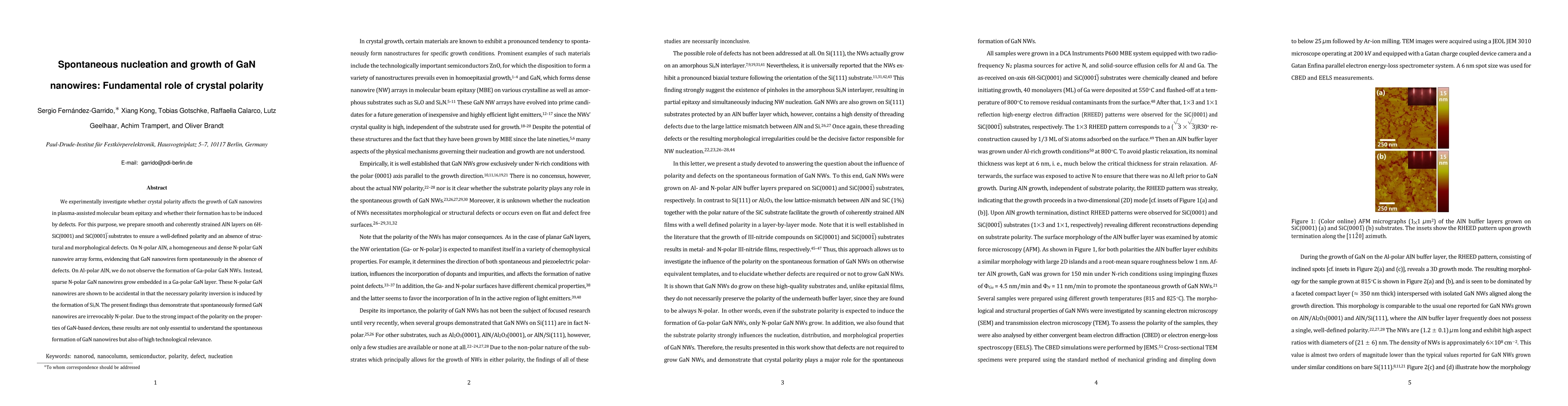
We experimentally investigate whether crystal polarity affects the growth of GaN nanowires in plasma-assisted molecular beam epitaxy and whether their formation has to be induced by defects. For thi...

Thumbnail for Molecular Beam Epitaxy of GaN Nanowires on Epitaxial Graphene
arXiv
Molecular Beam Epitaxy of GaN Nanowires on Epitaxial Graphene

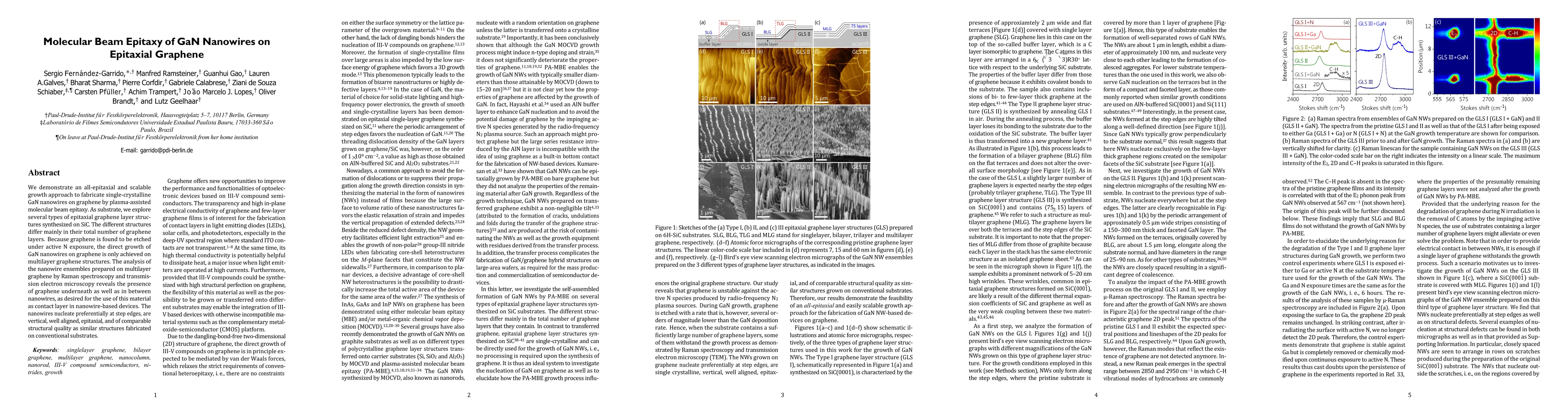
We demonstrate an all-epitaxial and scalable growth approach to fabricate single-crystalline GaN nanowires on graphene by plasma-assisted molecular beam epitaxy. As substrate, we explore several typ...

Thumbnail for Observation of dielectrically confined excitons in ultrathin GaN
  nanowires up to room temperature
arXiv
Observation of dielectrically confined excitons in ultrathin GaN nanowires up to room temperature

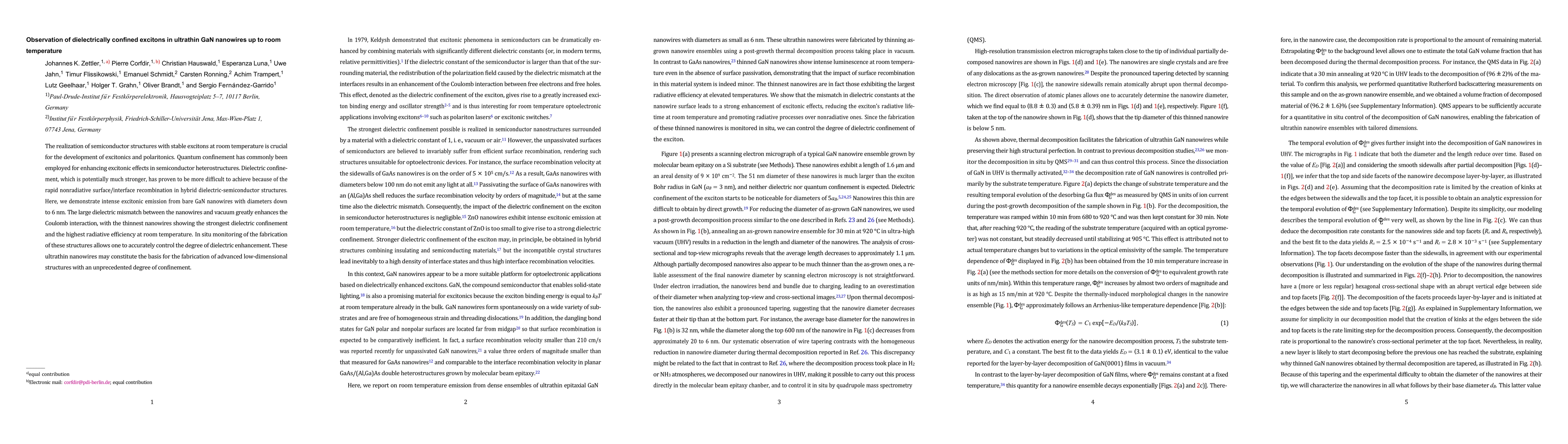
The realization of semiconductor structures with stable excitons at room temperature is crucial for the development of excitonics and polaritonics. Quantum confinement has commonly been employed for...

Thumbnail for Polarity-induced selective area epitaxy of GaN nanowires
arXiv
Polarity-induced selective area epitaxy of GaN nanowires

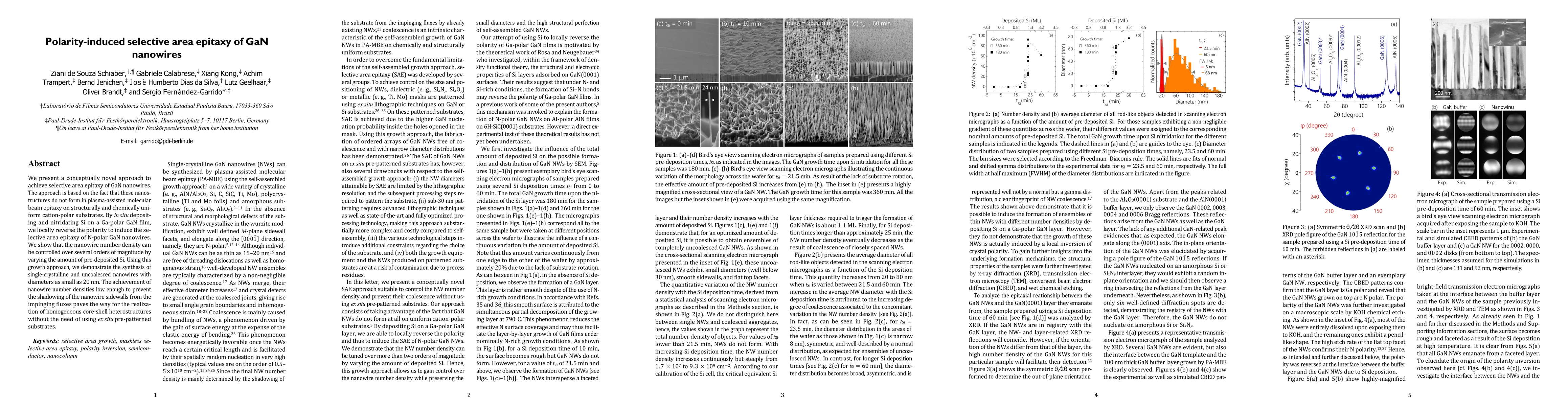
We present a conceptually novel approach to achieve selective area epitaxy of GaN nanowires. The approach is based on the fact that these nanostructures do not form in plasma-assisted molecular beam...

Thumbnail for X-ray scattering study of GaN nanowires grown on Ti/Al$_{2}$O$_{3}$ by
  molecular beam epitaxy
arXiv
X-ray scattering study of GaN nanowires grown on Ti/Al$_{2}$O$_{3}$ by molecular beam epitaxy

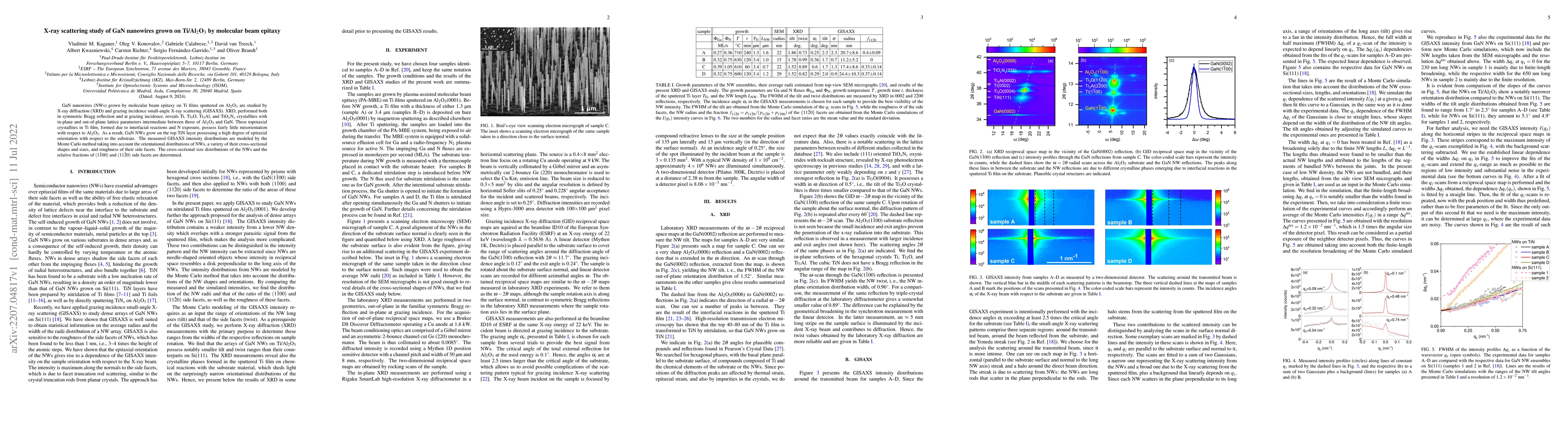
GaN nanowires (NWs) grown by molecular beam epitaxy on Ti films sputtered on Al$_{2}$O$_{3}$ are studied by X-ray diffraction (XRD) and grazing incidence small-angle X-ray scattering (GISAXS). XRD, ...

Thumbnail for Interface recombination in Ga- and N-polar GaN/(Al,Ga)N quantum wells
  grown by molecular beam epitaxy
arXiv
Interface recombination in Ga- and N-polar GaN/(Al,Ga)N quantum wells grown by molecular beam epitaxy

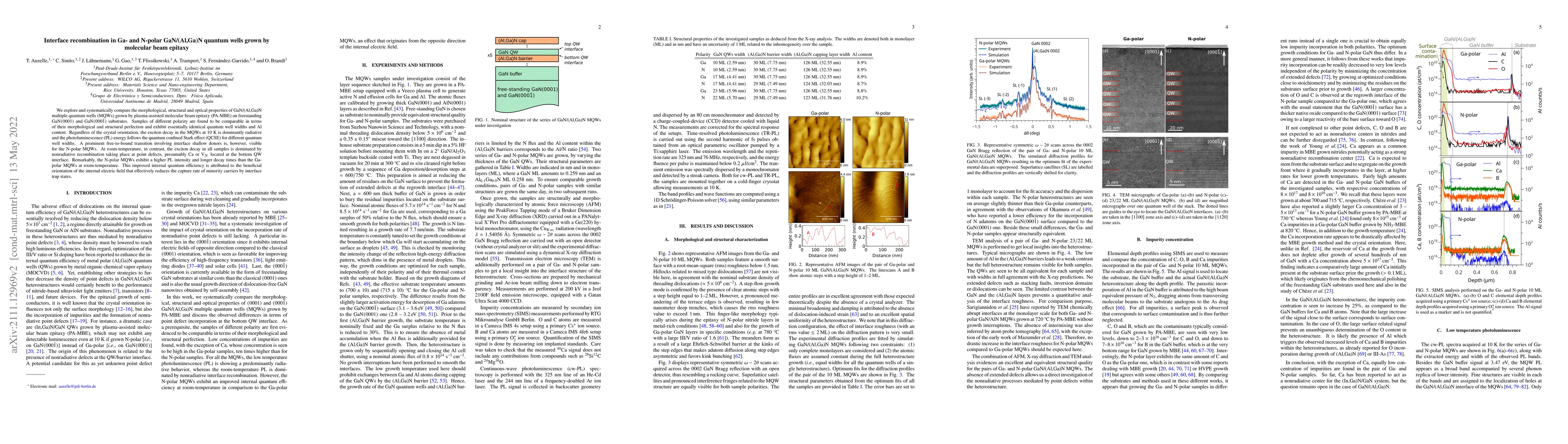
We explore and systematically compare the morphological, structural and optical properties of GaN/(Al,Ga)N multiple quantum wells (MQWs) grown by plasma-assisted molecular beam epitaxy (PA-MBE) on f...

Thumbnail for A growth diagram for chemical beam epitaxy of GaP$_{1-x}$N$_{x}$ alloys
  on nominally $(001)$-oriented GaP-on-Si substrates
arXiv
A growth diagram for chemical beam epitaxy of GaP$_{1-x}$N$_{x}$ alloys on nominally $(001)$-oriented GaP-on-Si substrates

The dilute-nitride ternary compound GaP$_{1-x}$N$_{x}$ is highly attractive to monolithically integrate pseudomorphic red light-emitting devices and photovoltaic cells with the standard Si technolog...

Thumbnail for Small-angle X-ray scattering from GaN nanowires on Si(111): facet
  truncation rods, facet roughness, and Porod's law
arXiv
Small-angle X-ray scattering from GaN nanowires on Si(111): facet truncation rods, facet roughness, and Porod's law

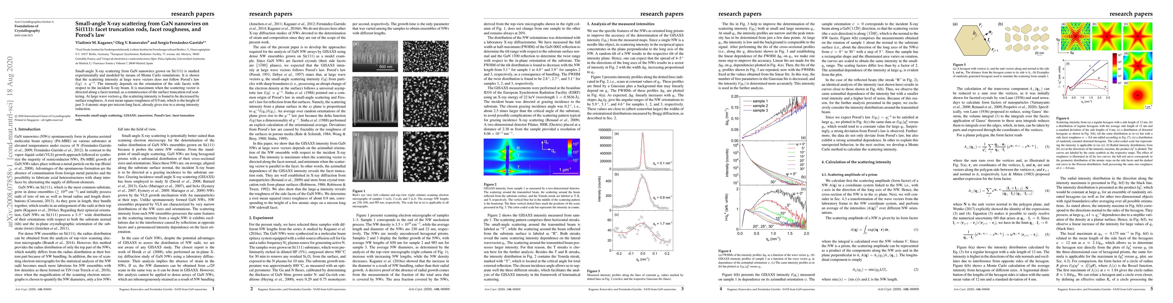
Small-angle X-ray scattering from GaN nanowires grown on Si(111) is studied experimentally and modeled by means of Monte Carlo simulations. It is shown that the scattering intensity at large wave ve...

Thumbnail for Electronic properties of air-exposed GaN$(1\bar{1}00)$ and $(0001)$
  surfaces after several device processing compatible cleaning steps
arXiv
Electronic properties of air-exposed GaN$(1\bar{1}00)$ and $(0001)$ surfaces after several device processing compatible cleaning steps

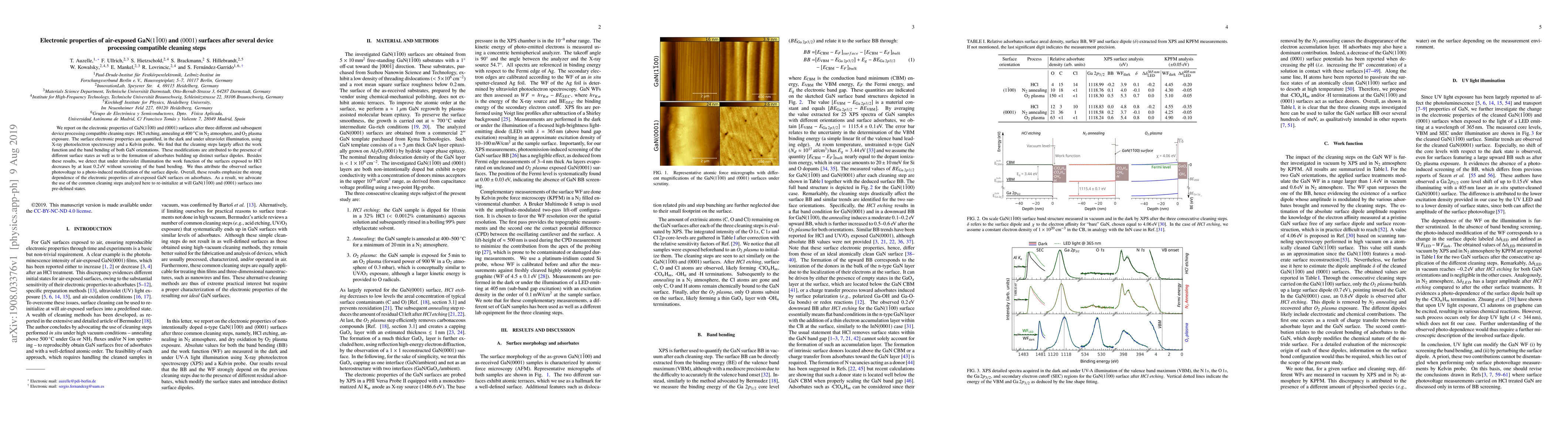
We report on the electronic properties of GaN$(1\bar{1}00)$ and $(0001)$ surfaces after three different and subsequent device processing compatible cleaning steps: HCl etching, annealing at $400$ $^...

This website uses cookies to ensure you get the best experience. Learn more