Academic Profile
Statistics
Similar Authors
Papers on arXiv
Analogue test structures were fabricated using the Tower Partners Semiconductor Co. CMOS 65 nm ISC process. The purpose was to characterise and qualify this process and to optimise the sensor for th...
Monolithic active pixel sensors (MAPS) produced in a 65 nm CMOS imaging technology are being investigated for applications in particle physics. The MAPS design has a small collection electrode chara...
Monolithic CMOS sensors in a 65 nm imaging technology are being investigated by the CERN EP Strategic R&D Programme on Technologies for Future Experiments for an application in particle physics. The...
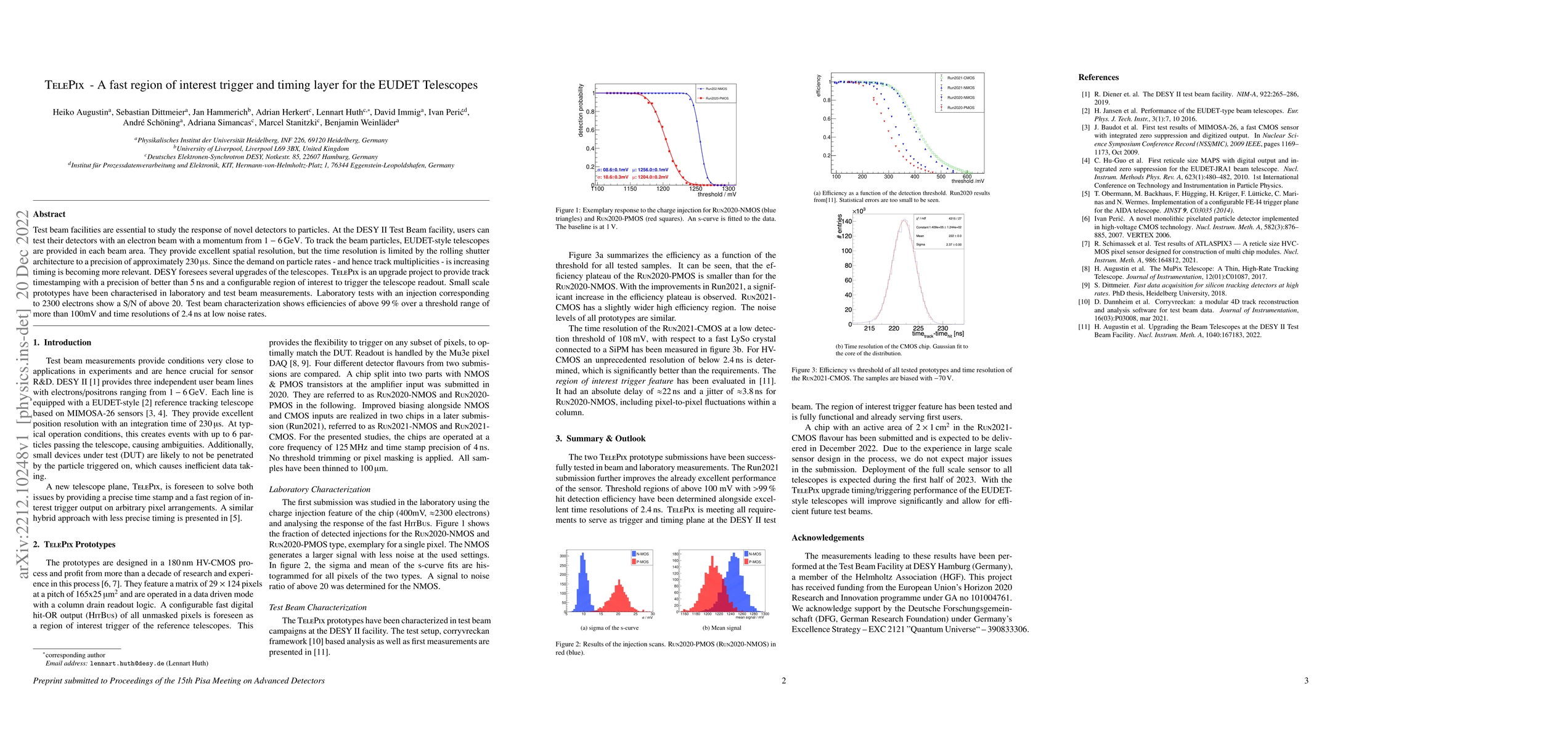
Test beam facilities are essential to study the response of novel detectors to particles. At the DESY II Test Beam facility, users can test their detectors with an electron beam with a momentum from...
A new generation of Monolithic Active Pixel Sensors (MAPS), produced in a 65 nm CMOS imaging process, promises higher densities of on-chip circuits and, for a given pixel size, more sophisticated in...
The Tangerine project aims to develop new state-of-the-art high-precision silicon detectors. Part of the project has the goal of developing a monolithic active pixel sensor using a novel 65 nm CMOS ...
The optimisation of the sensitive region of CMOS sensors with complex non-uniform electric fields requires precise simulations, and this can be achieved by a combination of electrostatic field simulat...
The goal of the TANGERINE project is to develop the next generation of monolithic silicon pixel detectors using a 65 nm CMOS imaging process, which offers a higher logic density and overall lower powe...
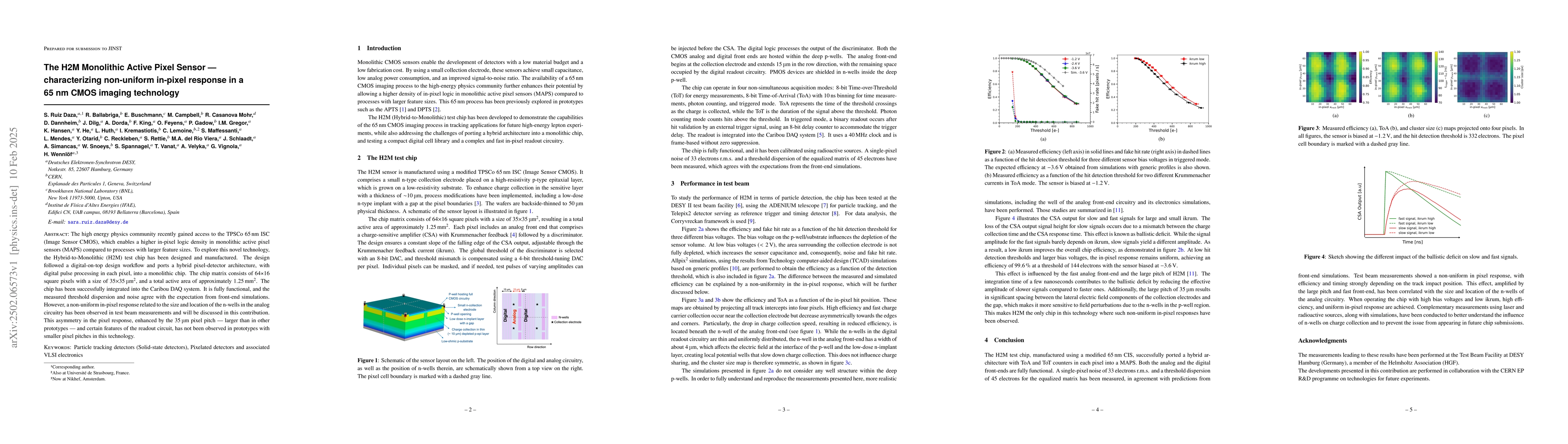
The high energy physics community recently gained access to the TPSCo 65 nm ISC (Image Sensor CMOS), which enables a higher in-pixel logic density in monolithic active pixel sensors (MAPS) compared to...
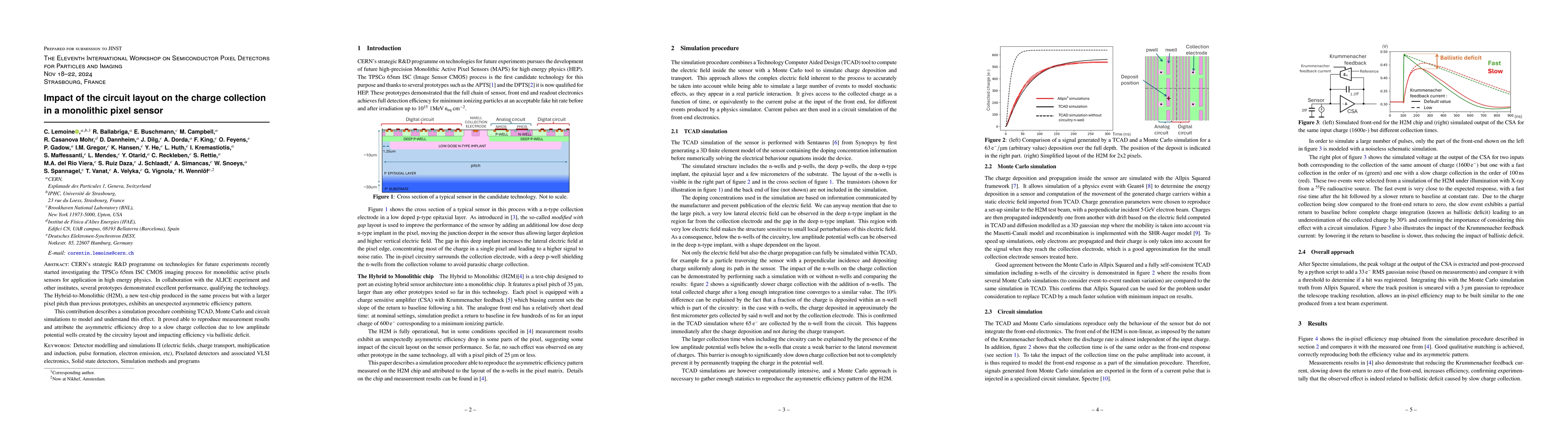
CERN's strategic R&D programme on technologies for future experiments recently started investigating the TPSCo 65nm ISC CMOS imaging process for monolithic active pixels sensors for application in hig...
The H2M (Hybrid-to-Monolithic) is a monolithic pixel sensor manufactured in a modified \SI{65}{\nano\meter}~CMOS imaging process with a small collection electrode. Its design addresses the challenges ...