Characterisation of analogue Monolithic Active Pixel Sensor test structures implemented in a 65 nm CMOS imaging process
Publication
Metrics
AI Quick Summary
This paper characterises analogue Monolithic Active Pixel Sensor test structures implemented in a 65 nm CMOS imaging process, evaluating various doping levels and pixel geometries under irradiation. Results show the technology's feasibility for high-energy physics and provide a foundation for future optimisations.
Paper Preview
Abstract
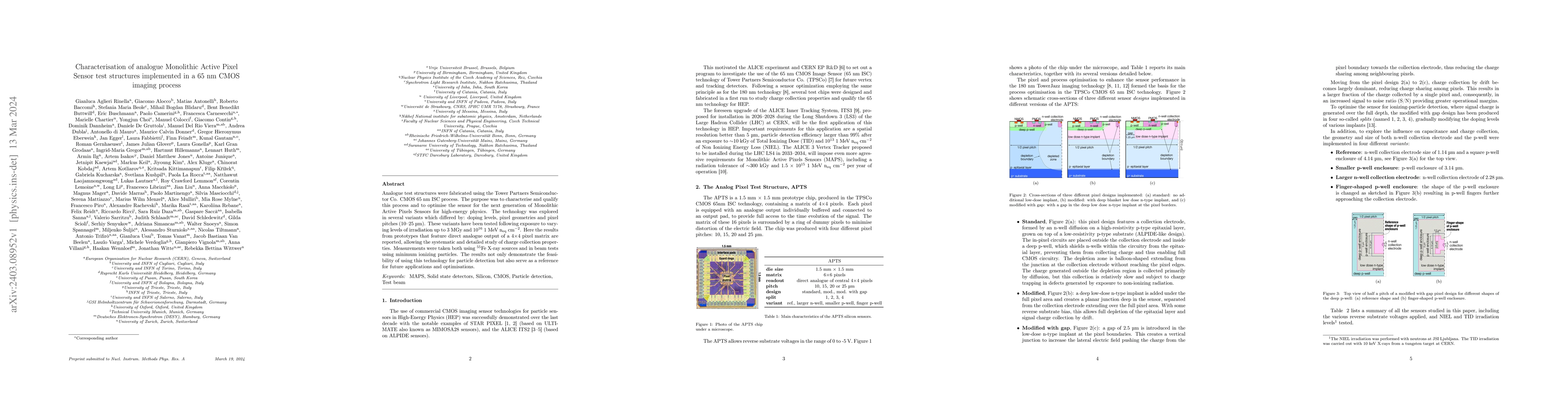
Analogue test structures were fabricated using the Tower Partners Semiconductor Co. CMOS 65 nm ISC process. The purpose was to characterise and qualify this process and to optimise the sensor for the next generation of Monolithic Active Pixels Sensors for high-energy physics. The technology was explored in several variants which differed by: doping levels, pixel geometries and pixel pitches (10-25 $\mu$m). These variants have been tested following exposure to varying levels of irradiation up to 3 MGy and $10^{16}$ 1 MeV n$_\text{eq}$ cm$^{-2}$. Here the results from prototypes that feature direct analogue output of a 4$\times$4 pixel matrix are reported, allowing the systematic and detailed study of charge collection properties. Measurements were taken both using $^{55}$Fe X-ray sources and in beam tests using minimum ionizing particles. The results not only demonstrate the feasibility of using this technology for particle detection but also serve as a reference for future applications and optimisations.
AI Key Findings
Get AI-generated insights about this paper's methodology, results, significance, and more — seven facets brought into focus.
Impact
Paper Details
Authors
PDF Preview
Key Terms
Citation Network
Current paper (gray), citations (green), references (blue)
Display is limited for performance on very large graphs.
Discussion 0