Academic Profile
Statistics
Similar Authors
Papers on arXiv
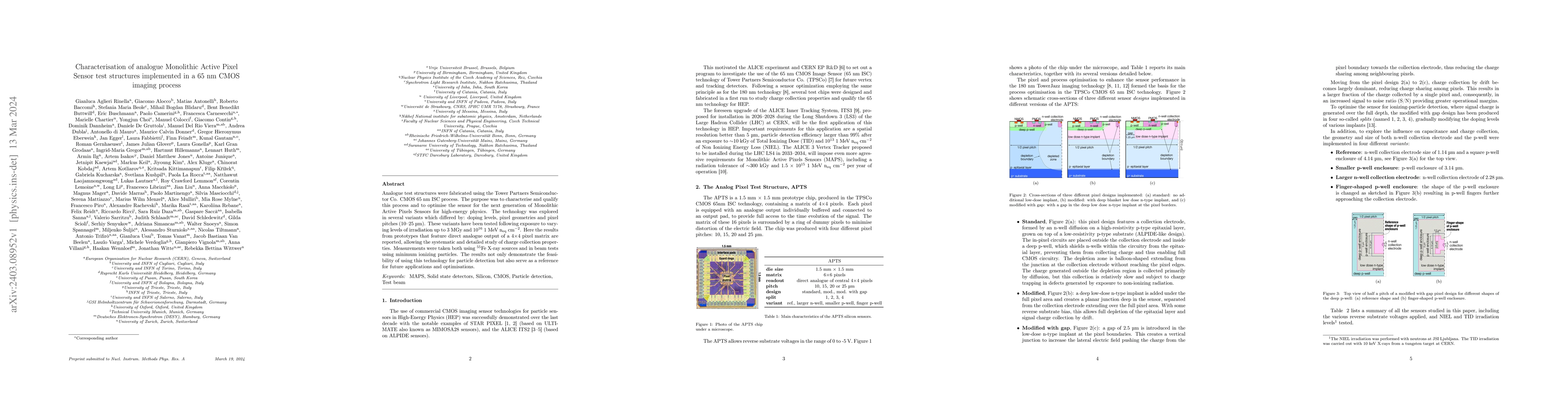
Analogue test structures were fabricated using the Tower Partners Semiconductor Co. CMOS 65 nm ISC process. The purpose was to characterise and qualify this process and to optimise the sensor for th...
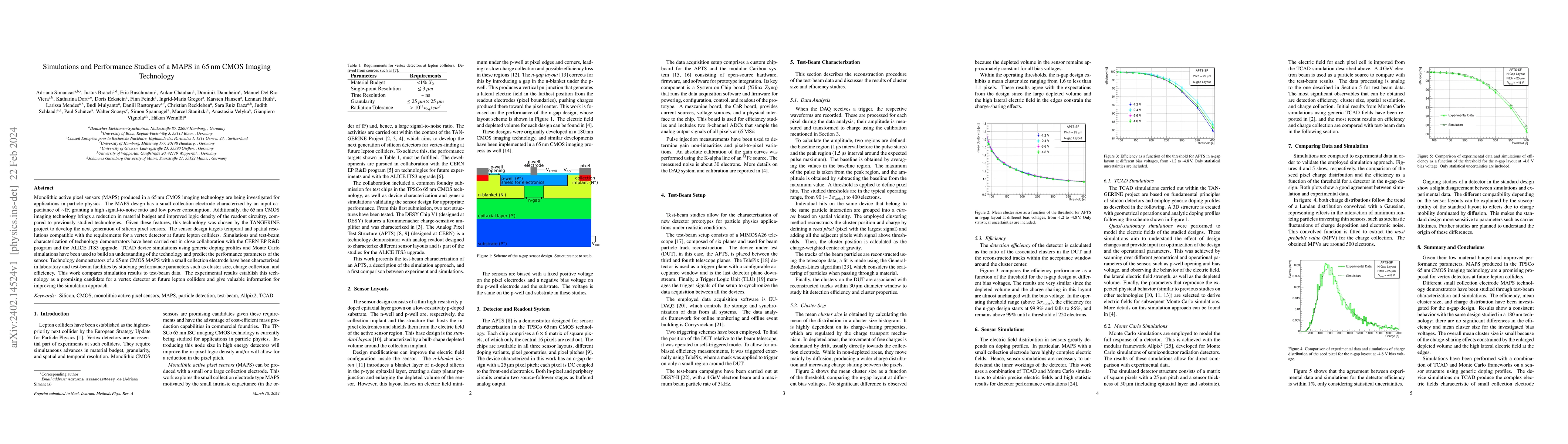
Monolithic active pixel sensors (MAPS) produced in a 65 nm CMOS imaging technology are being investigated for applications in particle physics. The MAPS design has a small collection electrode chara...
Monolithic CMOS sensors in a 65 nm imaging technology are being investigated by the CERN EP Strategic R&D Programme on Technologies for Future Experiments for an application in particle physics. The...
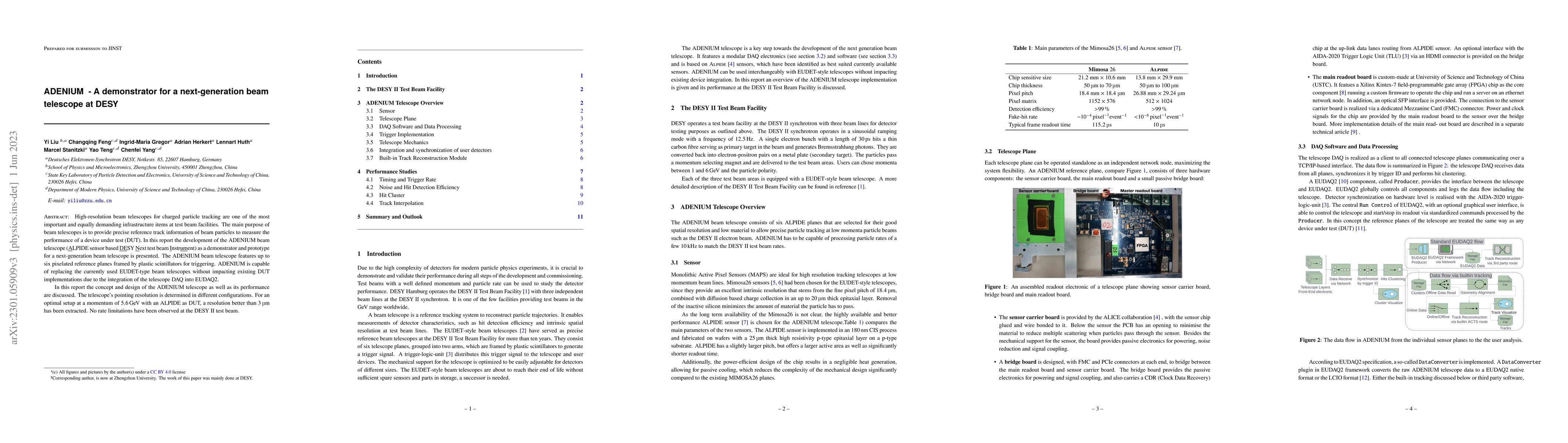
High-resolution beam telescopes for charged particle tracking are one of the most important and equally demanding infrastructure items at test beam facilities. The main purpose of beam telescopes is...
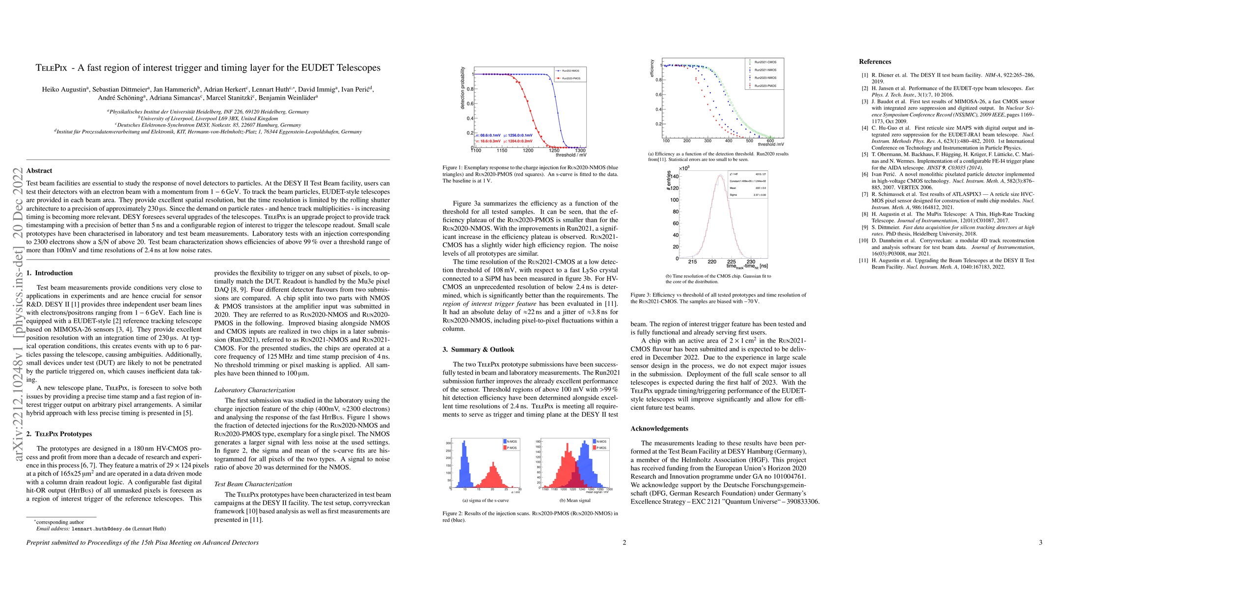
Test beam facilities are essential to study the response of novel detectors to particles. At the DESY II Test Beam facility, users can test their detectors with an electron beam with a momentum from...
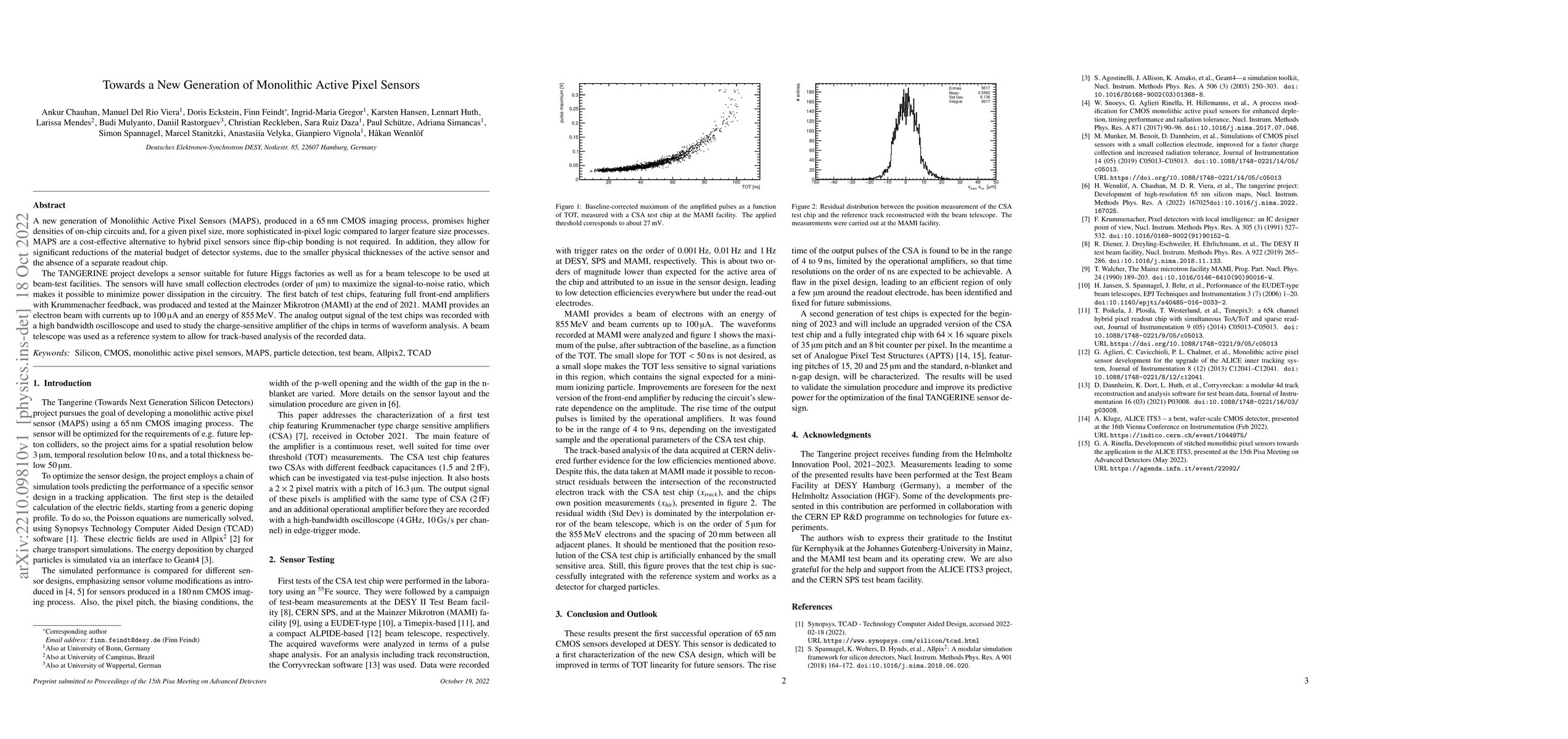
A new generation of Monolithic Active Pixel Sensors (MAPS), produced in a 65 nm CMOS imaging process, promises higher densities of on-chip circuits and, for a given pixel size, more sophisticated in...
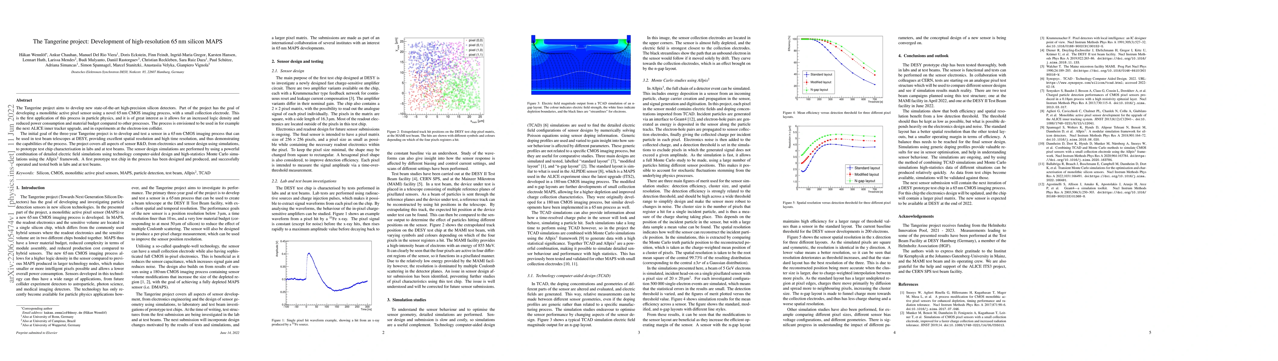
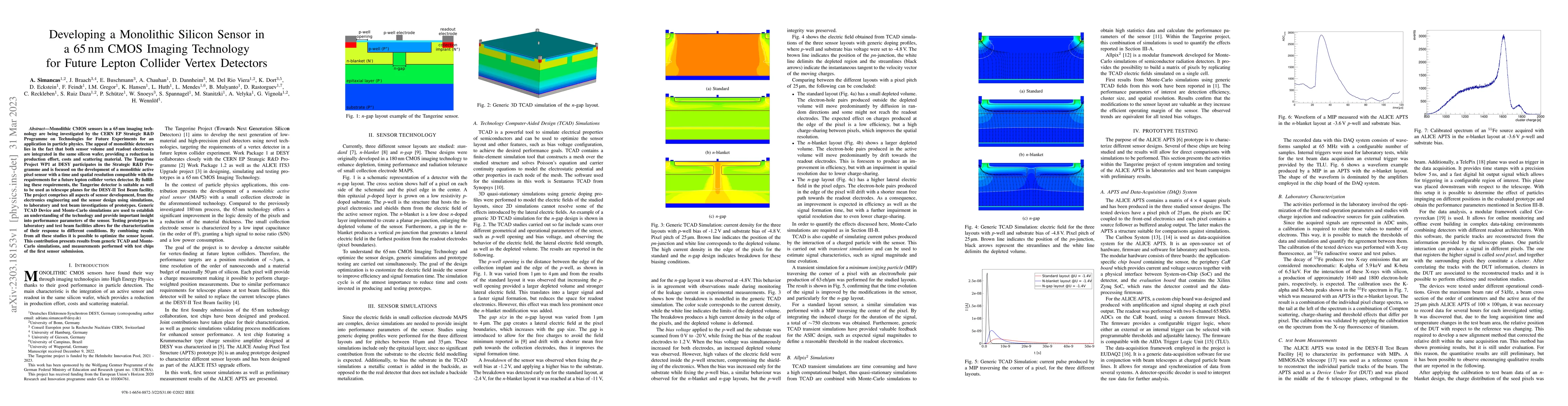
The Tangerine project aims to develop new state-of-the-art high-precision silicon detectors. Part of the project has the goal of developing a monolithic active pixel sensor using a novel 65 nm CMOS ...
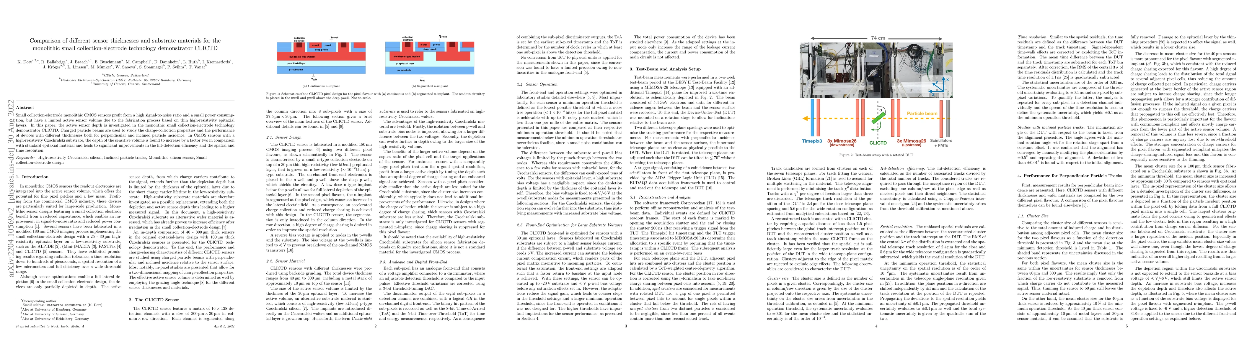
Small collection-electrode monolithic CMOS sensors profit from a high signal-to-noise ratio and a small power consumption, but have a limited active sensor volume due to the fabrication process base...
An ever-increasing demand for high-performance silicon sensors requires complex sensor designs that are challenging to simulate and model. The combination of electrostatic finite element simulations...
Stringent requirements are posed on the the next generations of vertex and tracking detectors for high-energy physics experiments to reach the foreseen physics goals. A large variety of silicon pixe...
The optimisation of the sensitive region of CMOS sensors with complex non-uniform electric fields requires precise simulations, and this can be achieved by a combination of electrostatic field simulat...
The goal of the TANGERINE project is to develop the next generation of monolithic silicon pixel detectors using a 65 nm CMOS imaging process, which offers a higher logic density and overall lower powe...
The high energy physics community recently gained access to the TPSCo 65 nm ISC (Image Sensor CMOS), which enables a higher in-pixel logic density in monolithic active pixel sensors (MAPS) compared to...
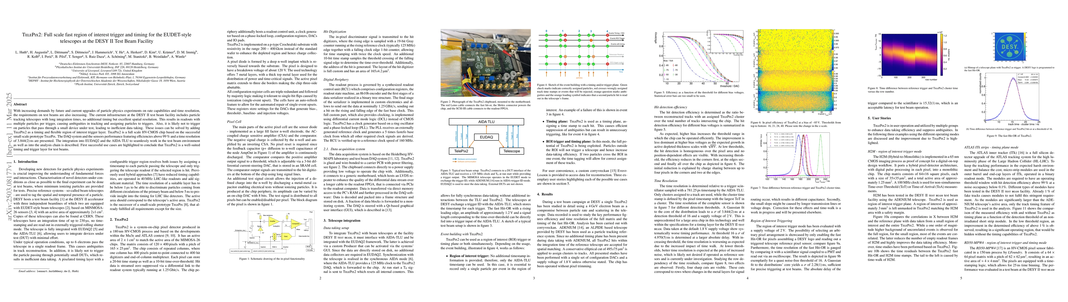
With increasing demands by future and current upgrades of particle physics experiments on rate capabilities and time resolution, the requirements on test beams are also increasing. The current infrast...
Muons offer a unique opportunity to build a compact high-energy electroweak collider at the 10 TeV scale. A Muon Collider enables direct access to the underlying simplicity of the Standard Model and u...
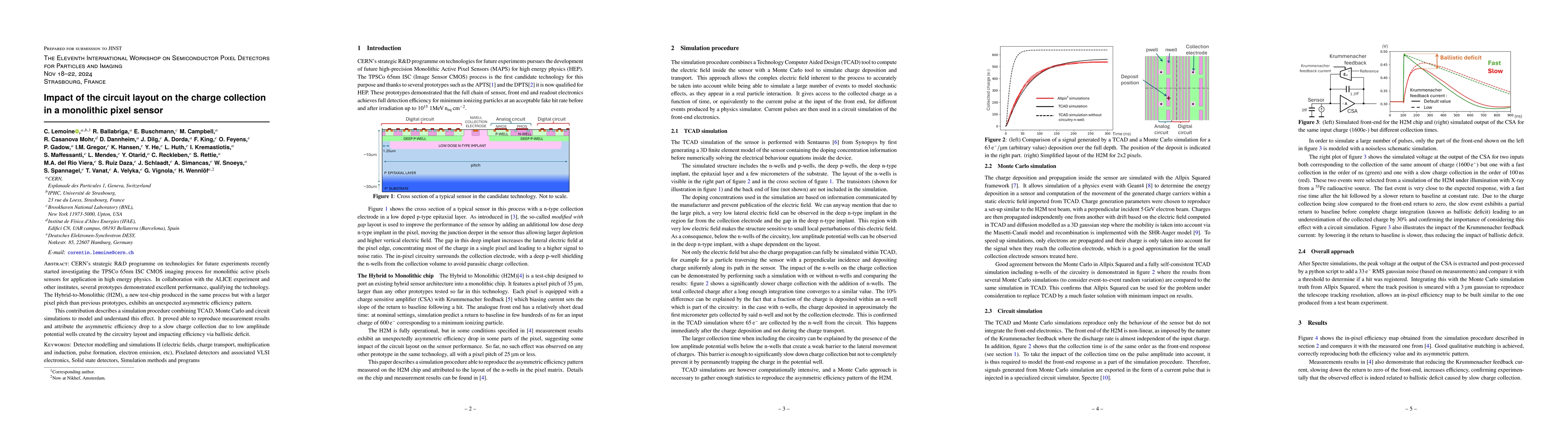
CERN's strategic R&D programme on technologies for future experiments recently started investigating the TPSCo 65nm ISC CMOS imaging process for monolithic active pixels sensors for application in hig...
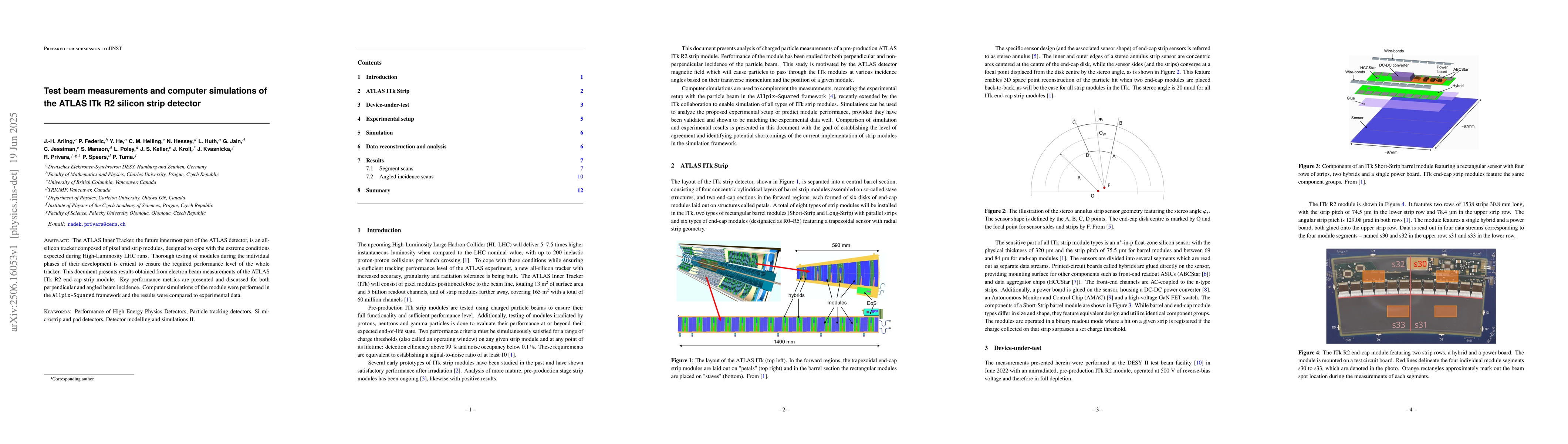
The ATLAS Inner Tracker, the future innermost part of the ATLAS detector, is an all-silicon tracker composed of pixel and strip modules, designed to cope with the extreme conditions expected during Hi...
This document is comprised of a collection of consolidated parameters for the key parts of the muon collider. These consolidated parameters follow on from the October 2024 Preliminary Parameters Repor...
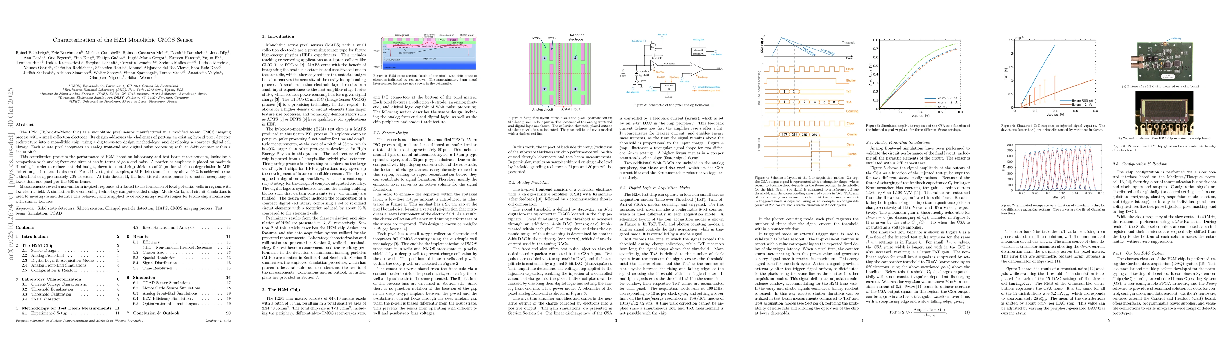
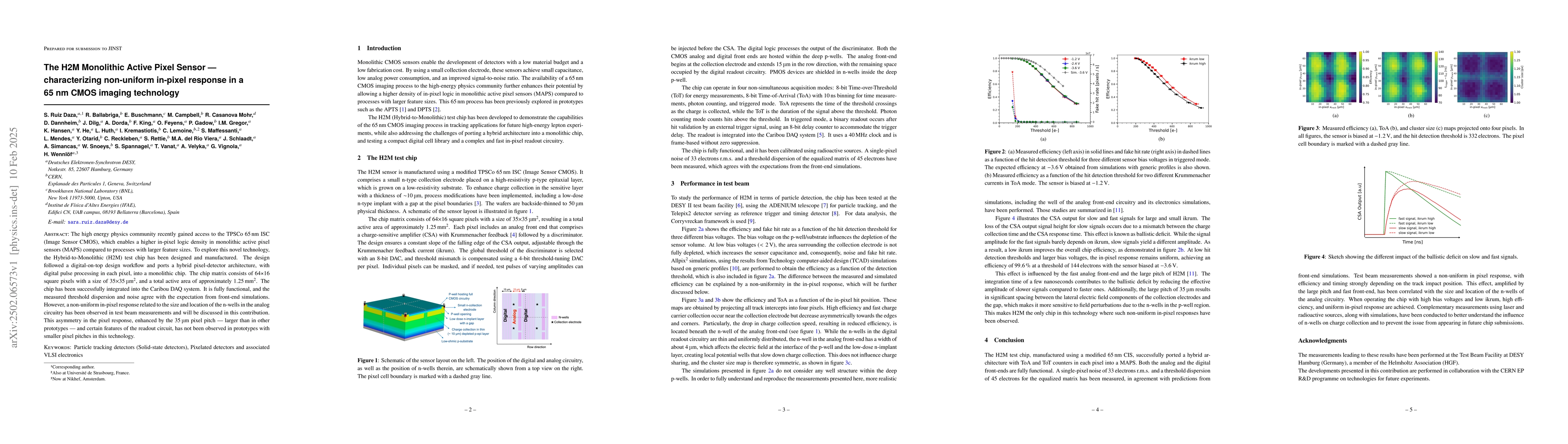
The H2M (Hybrid-to-Monolithic) is a monolithic pixel sensor manufactured in a modified \SI{65}{\nano\meter}~CMOS imaging process with a small collection electrode. Its design addresses the challenges ...

The inner tracking system of the ATLAS experiment will be upgraded to a full silicon detector in 2030 for HL-LHC. The new tracking system is called ITk, the Inner Tracker. It is required to be operabl...
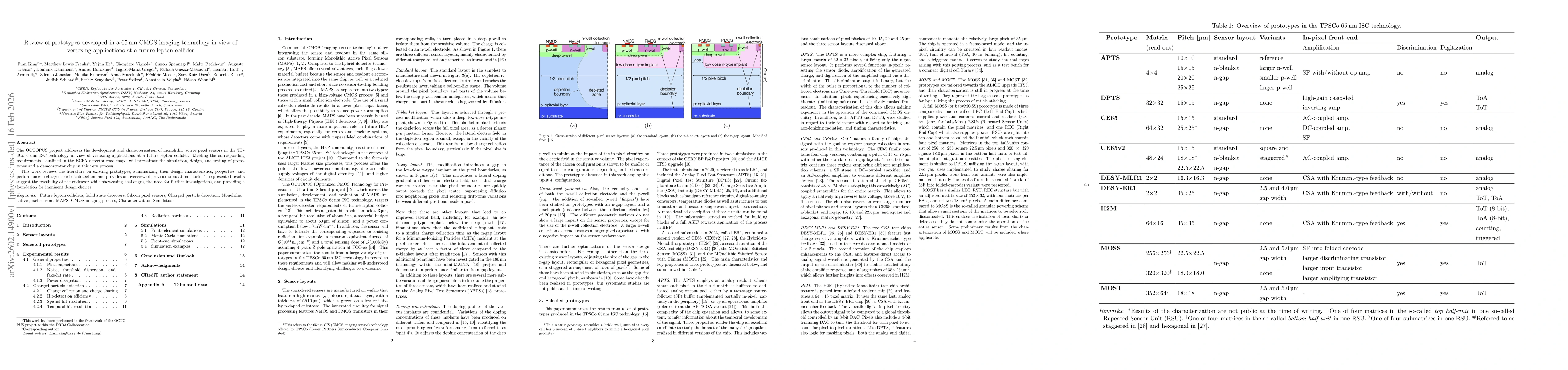
The OCTOPUS project addresses the development and characterization of monolithic active pixel sensors in the TPSCo 65 nm ISC technology in view of vertexing applications at a future lepton collider. M...