Dominik Dannheim

23 papers on arXiv

Academic Profile

Name: D. Dannheim
Total Papers: 8

Statistics

arXiv Papers 23
Total Publications 8

Papers on arXiv

Thumbnail for Commissioning and Performance of the ATLAS Liquid Argon Calorimeters

Commissioning and Performance of the ATLAS Liquid Argon Calorimeters

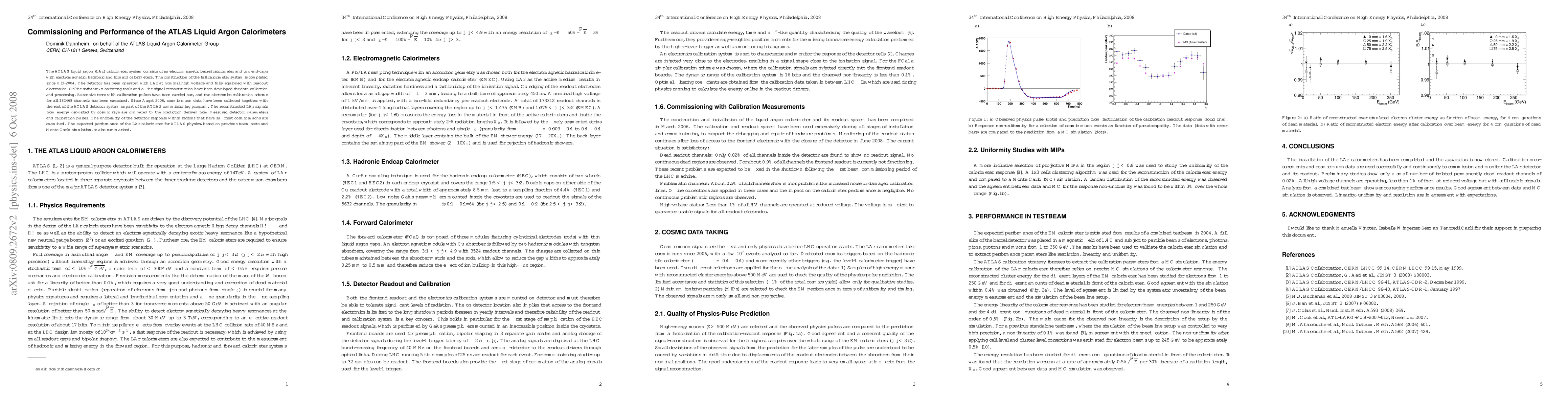
The ATLAS liquid argon (LAr) calorimeter system consists of an electromagnetic barrel calorimeter and two end-caps with electromagnetic, hadronic and forward calorimeters. The construction of the fu...

Thumbnail for Characterisation of analogue Monolithic Active Pixel Sensor test
  structures implemented in a 65 nm CMOS imaging process

Characterisation of analogue Monolithic Active Pixel Sensor test structures implemented in a 65 nm CMOS imaging process

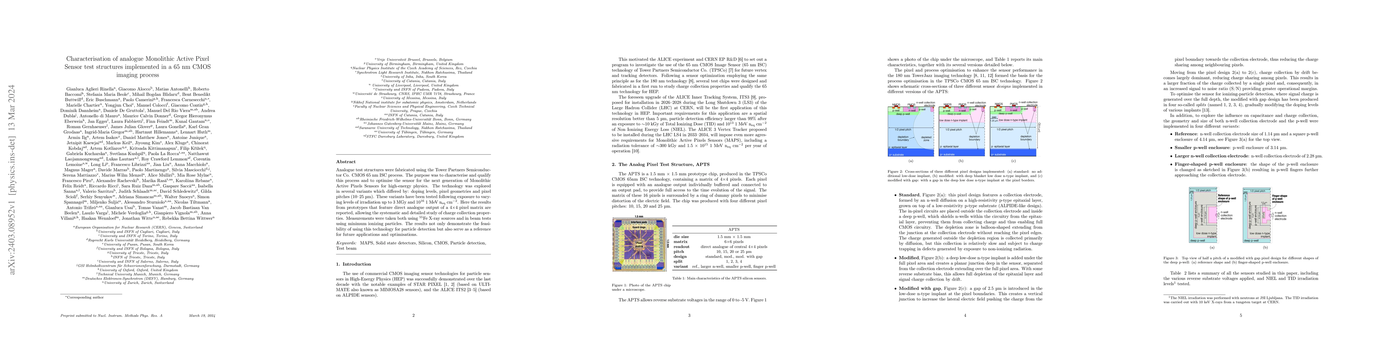
Analogue test structures were fabricated using the Tower Partners Semiconductor Co. CMOS 65 nm ISC process. The purpose was to characterise and qualify this process and to optimise the sensor for th...

Thumbnail for Simulations and Performance Studies of a MAPS in 65 nm CMOS Imaging
  Technology

Simulations and Performance Studies of a MAPS in 65 nm CMOS Imaging Technology

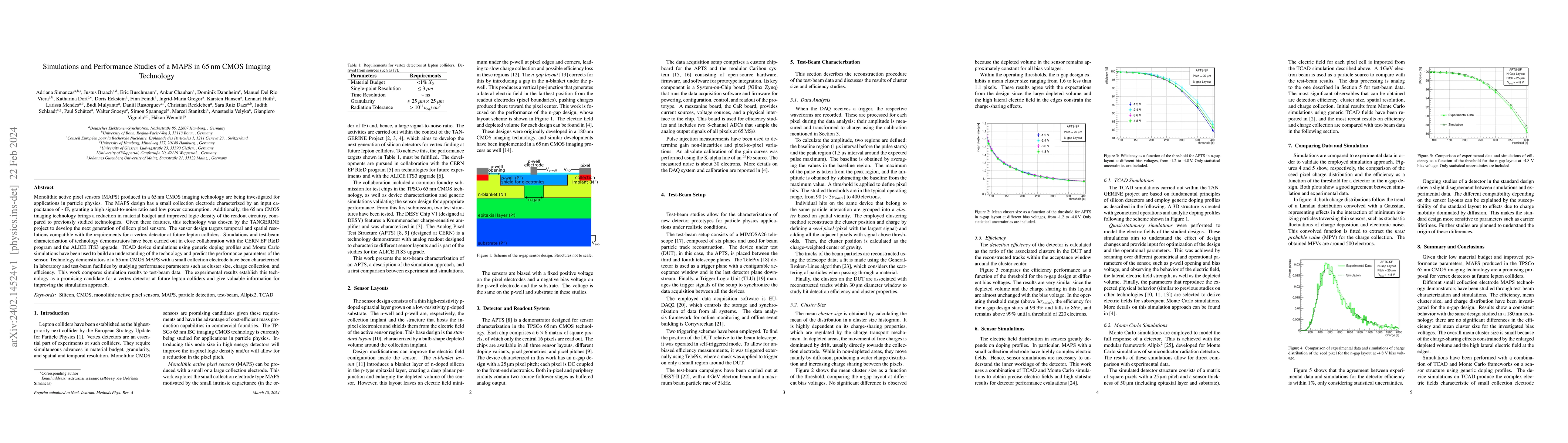
Monolithic active pixel sensors (MAPS) produced in a 65 nm CMOS imaging technology are being investigated for applications in particle physics. The MAPS design has a small collection electrode chara...

Thumbnail for Pixel detector hybridization and integration with anisotropic conductive
  adhesives

Pixel detector hybridization and integration with anisotropic conductive adhesives

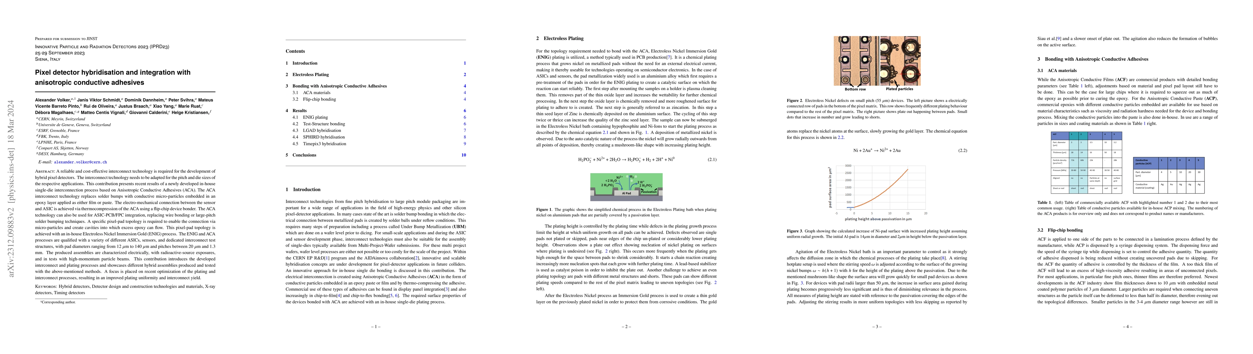
A reliable and cost-effective interconnect technology is required for the development of hybrid pixel detectors. The interconnect technology needs to be adapted for the pitch and die sizes of the re...

Thumbnail for Test-beam Performance Results of the FASTPIX Sub-Nanosecond CMOS Pixel
  Sensor Demonstrator

Test-beam Performance Results of the FASTPIX Sub-Nanosecond CMOS Pixel Sensor Demonstrator

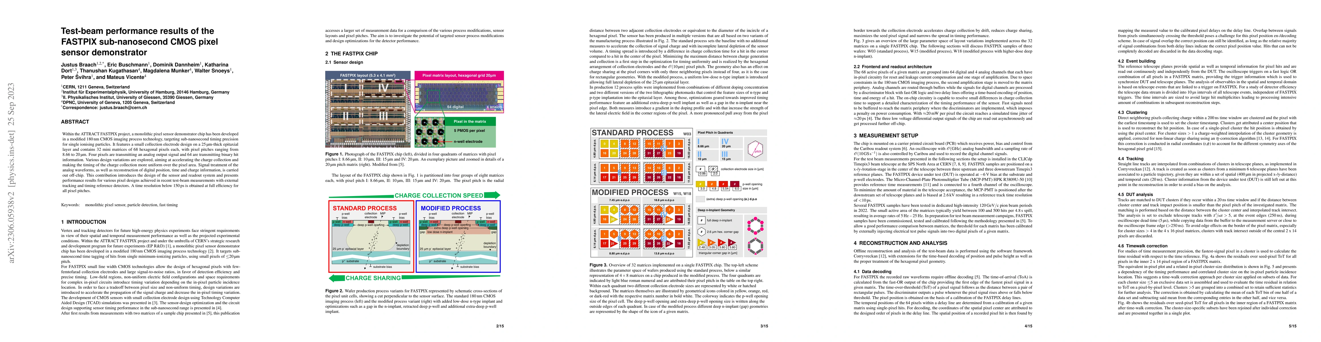
Within the ATTRACT FASTPIX project, a monolithic pixel sensor demonstrator chip has been developed in a modified 180 nm CMOS imaging process technology, targeting sub-nanosecond timing precision for...

Thumbnail for Developing a Monolithic Silicon Sensor in a 65 nm CMOS Imaging
  Technology for Future Lepton Collider Vertex Detectors

Developing a Monolithic Silicon Sensor in a 65 nm CMOS Imaging Technology for Future Lepton Collider Vertex Detectors

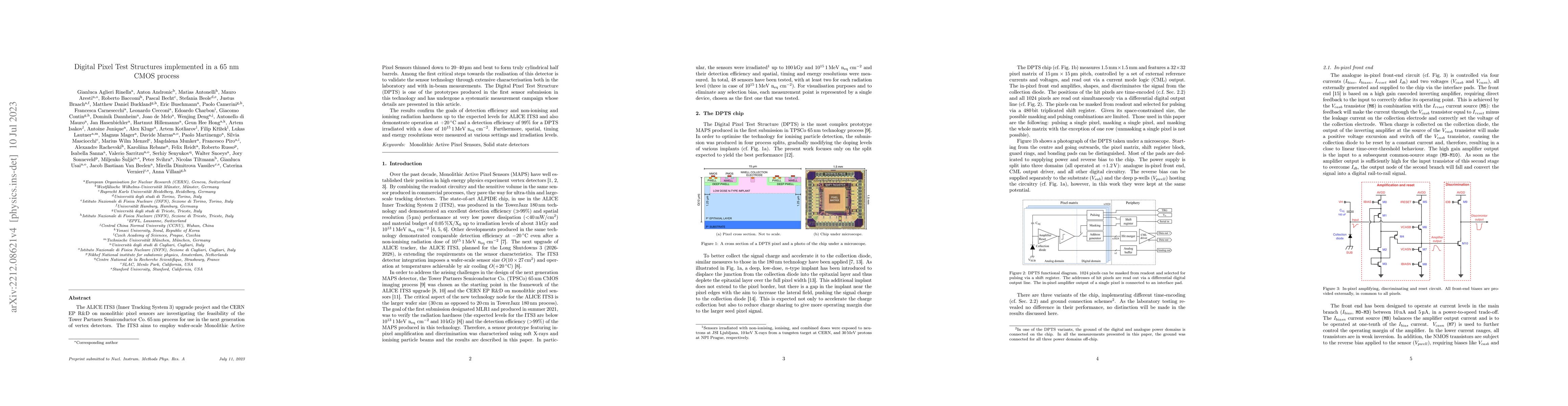
Monolithic CMOS sensors in a 65 nm imaging technology are being investigated by the CERN EP Strategic R&D Programme on Technologies for Future Experiments for an application in particle physics. The...

Thumbnail for Digital Pixel Test Structures implemented in a 65 nm CMOS process

Digital Pixel Test Structures implemented in a 65 nm CMOS process

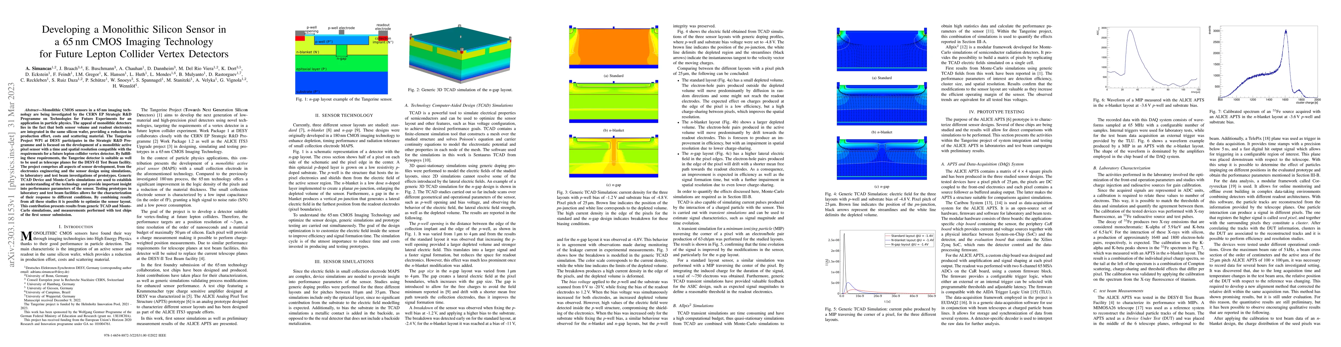
The ALICE ITS3 (Inner Tracking System 3) upgrade project and the CERN EP R&D on monolithic pixel sensors are investigating the feasibility of the Tower Partners Semiconductor Co. 65 nm process for u...

Thumbnail for Development of novel single-die hybridisation processes for small-pitch
  pixel detectors

Development of novel single-die hybridisation processes for small-pitch pixel detectors

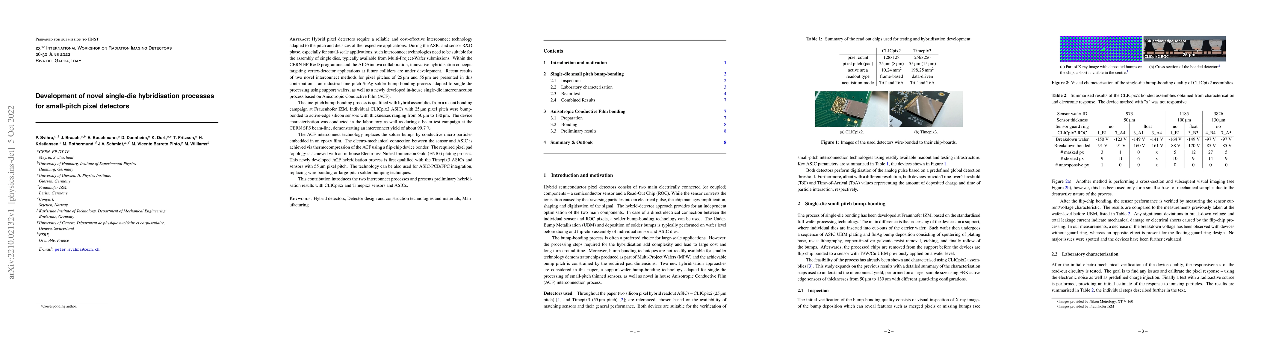
Hybrid pixel detectors require a reliable and cost-effective interconnect technology adapted to the pitch and die sizes of the respective applications. During the ASIC and sensor R\&D phase, especia...

Thumbnail for Comparison of different sensor thicknesses and substrate materials for
  the monolithic small collection-electrode technology demonstrator CLICTD

Comparison of different sensor thicknesses and substrate materials for the monolithic small collection-electrode technology demonstrator CLICTD

Small collection-electrode monolithic CMOS sensors profit from a high signal-to-noise ratio and a small power consumption, but have a limited active sensor volume due to the fabrication process base...

Thumbnail for Transient Monte Carlo Simulations for the Optimisation and
  Characterisation of Monolithic Silicon Sensors

Transient Monte Carlo Simulations for the Optimisation and Characterisation of Monolithic Silicon Sensors

An ever-increasing demand for high-performance silicon sensors requires complex sensor designs that are challenging to simulate and model. The combination of electrostatic finite element simulations...

Thumbnail for Combining TCAD and Monte Carlo Methods to Simulate CMOS Pixel Sensors
  with a Small Collection Electrode using the Allpix Squared Framework

Combining TCAD and Monte Carlo Methods to Simulate CMOS Pixel Sensors with a Small Collection Electrode using the Allpix Squared Framework

Combining electrostatic field simulations with Monte Carlo methods enables realistic modeling of the detector response for novel monolithic silicon detectors with strongly non-linear electric fields...

Thumbnail for Laboratory and beam-test performance study of a 55$~μ$m pitch iLGAD
  sensor bonded to a Timepix3 readout chip

Laboratory and beam-test performance study of a 55$~μ$m pitch iLGAD sensor bonded to a Timepix3 readout chip

This contribution reports on characterisation results of a large-area (2$~\mathrm{cm}^2$) small pitch (55$~\mu$m) inverse Low-Gain Avalanche Detector (iLGAD), bonded to a Timepix3 readout chip. The il...

Thumbnail for Simulating Monolithic Active Pixel Sensors: A Technology-Independent
  Approach Using Generic Doping Profiles

Simulating Monolithic Active Pixel Sensors: A Technology-Independent Approach Using Generic Doping Profiles

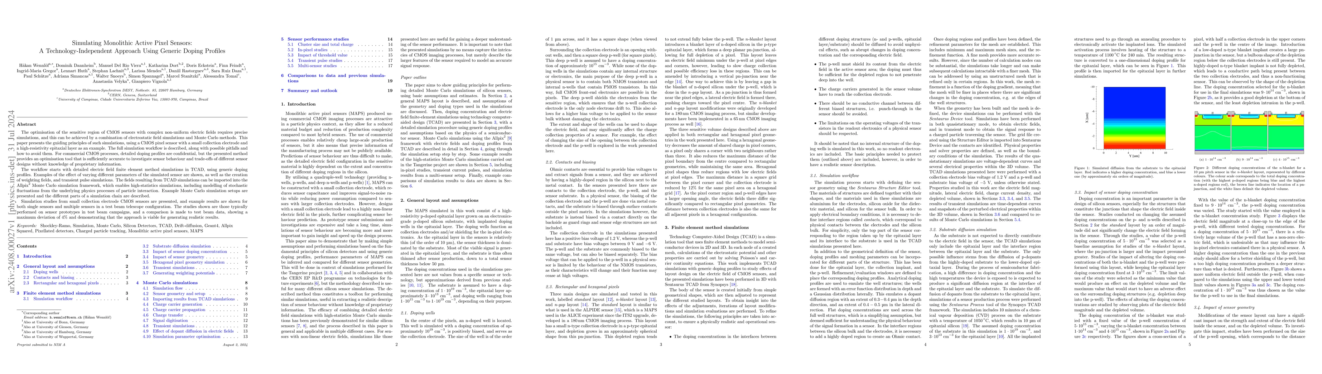
The optimisation of the sensitive region of CMOS sensors with complex non-uniform electric fields requires precise simulations, and this can be achieved by a combination of electrostatic field simulat...

Thumbnail for Transient studies using a TCAD and Allpix Squared combination approach

Transient studies using a TCAD and Allpix Squared combination approach

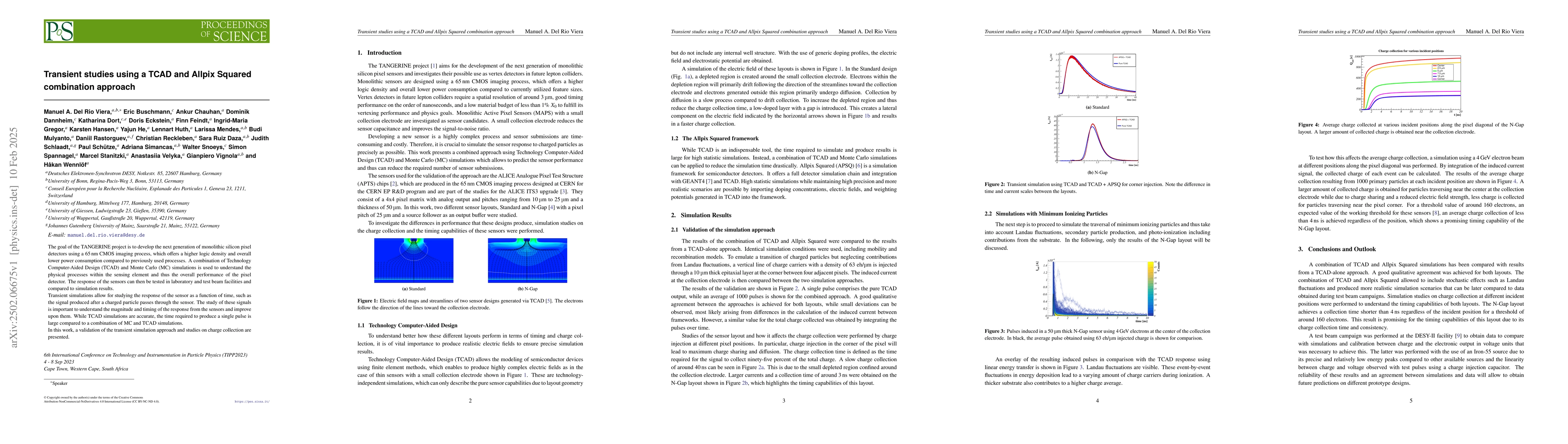
The goal of the TANGERINE project is to develop the next generation of monolithic silicon pixel detectors using a 65 nm CMOS imaging process, which offers a higher logic density and overall lower powe...

Thumbnail for The H2M Monolithic Active Pixel Sensor -- characterizing non-uniform
  in-pixel response in a 65 nm CMOS imaging technology

The H2M Monolithic Active Pixel Sensor -- characterizing non-uniform in-pixel response in a 65 nm CMOS imaging technology

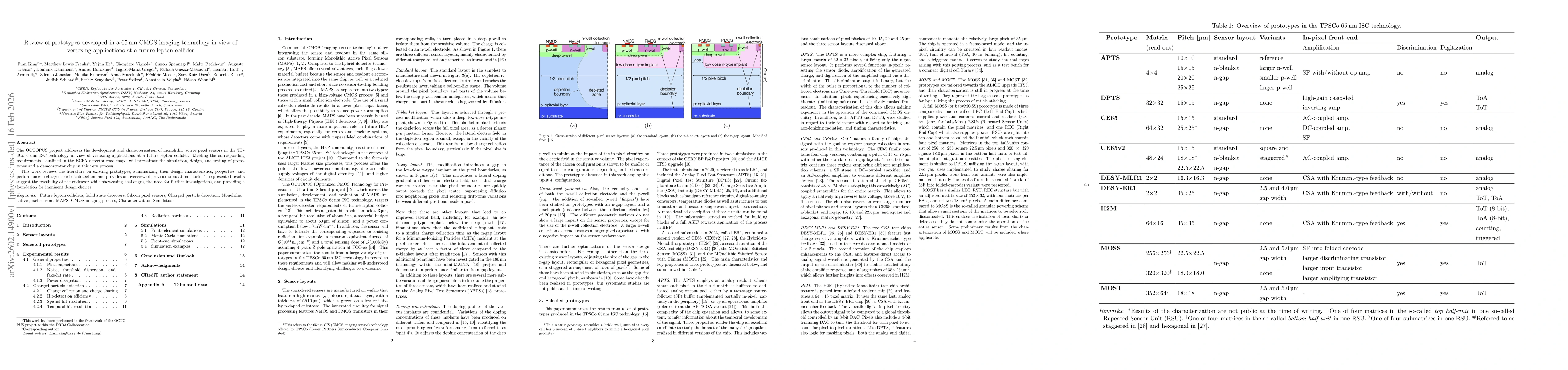
The high energy physics community recently gained access to the TPSCo 65 nm ISC (Image Sensor CMOS), which enables a higher in-pixel logic density in monolithic active pixel sensors (MAPS) compared to...

Thumbnail for Caribou -- A versatile data acquisition system for silicon pixel
  detector prototyping

Caribou -- A versatile data acquisition system for silicon pixel detector prototyping

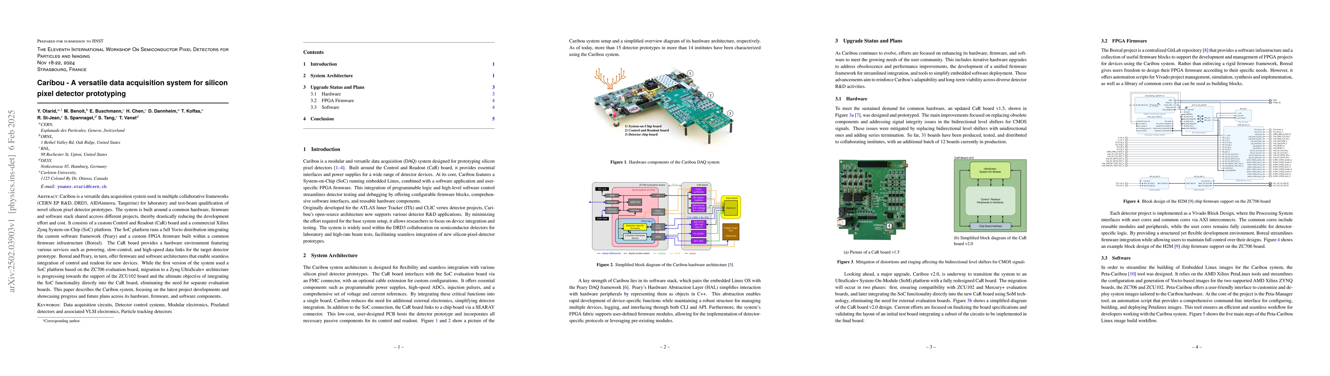
Caribou is a versatile data acquisition system used in multiple collaborative frameworks (CERN EP R&D, DRD3, AIDAinnova, Tangerine) for laboratory and test-beam qualification of novel silicon pixel de...

Thumbnail for Impact of the circuit layout on the charge collection in a monolithic
  pixel sensor

Impact of the circuit layout on the charge collection in a monolithic pixel sensor

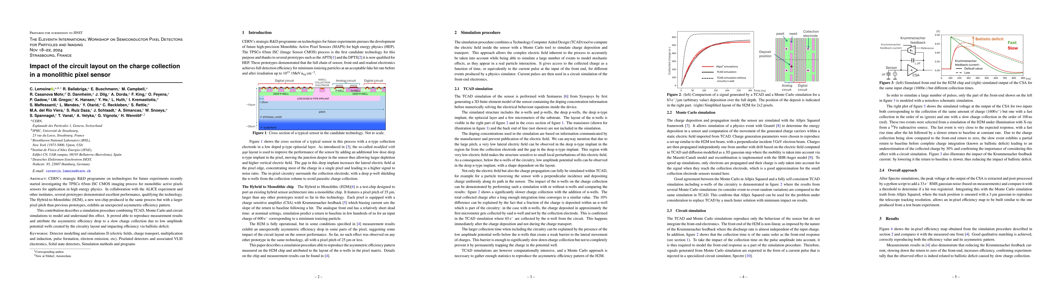
CERN's strategic R&D programme on technologies for future experiments recently started investigating the TPSCo 65nm ISC CMOS imaging process for monolithic active pixels sensors for application in hig...

Thumbnail for The Compact Linear e$^+$e$^-$ Collider (CLIC)

The Compact Linear e$^+$e$^-$ Collider (CLIC)

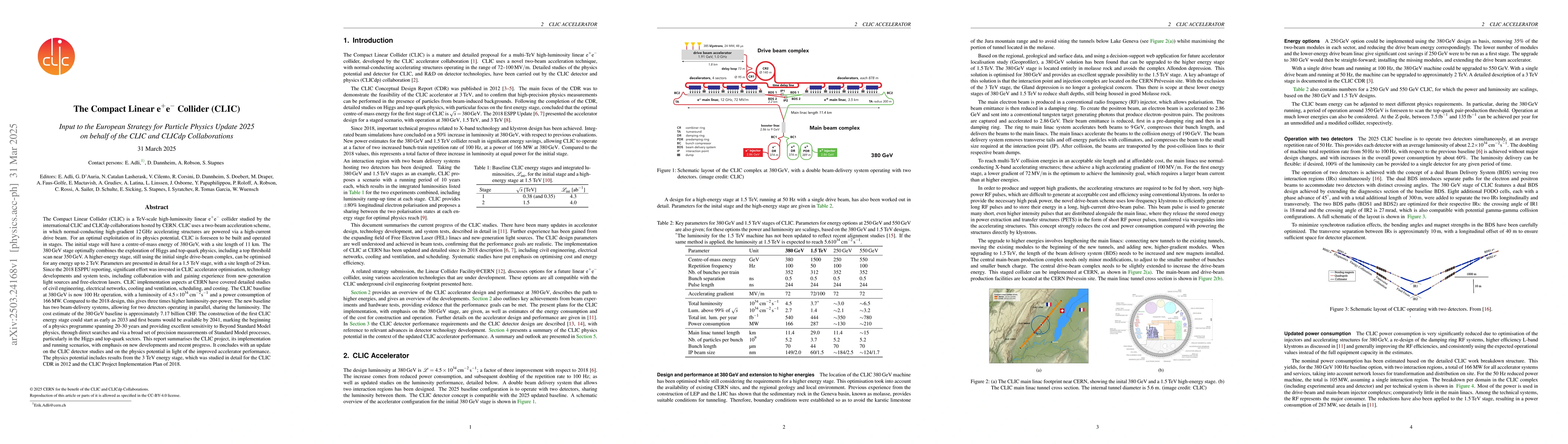
The Compact Linear Collider (CLIC) is a TeV-scale high-luminosity linear e$^+$e$^-$ collider studied by the international CLIC and CLICdp collaborations. CLIC uses a two-beam acceleration scheme, in w...

Thumbnail for Further Characterisation of Digital Pixel Test Structures Implemented in
  a 65 nm CMOS Process

Further Characterisation of Digital Pixel Test Structures Implemented in a 65 nm CMOS Process

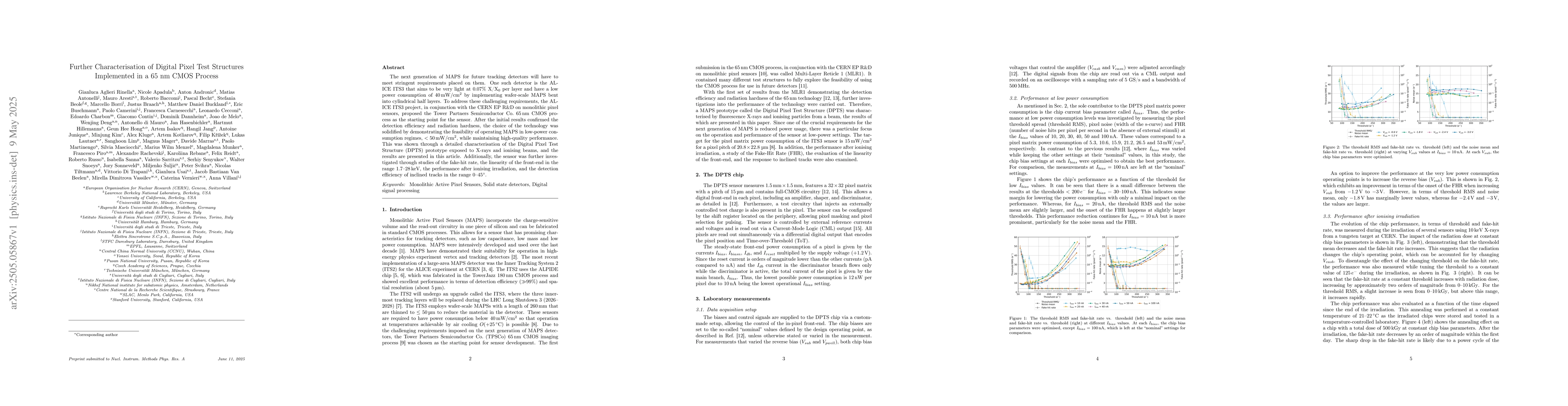
The next generation of MAPS for future tracking detectors will have to meet stringent requirements placed on them. One such detector is the ALICE ITS3 that aims to be very light at 0.07% X/X$_{0}$ per...

Thumbnail for Characterization of the H2M Monolithic CMOS Sensor

Characterization of the H2M Monolithic CMOS Sensor

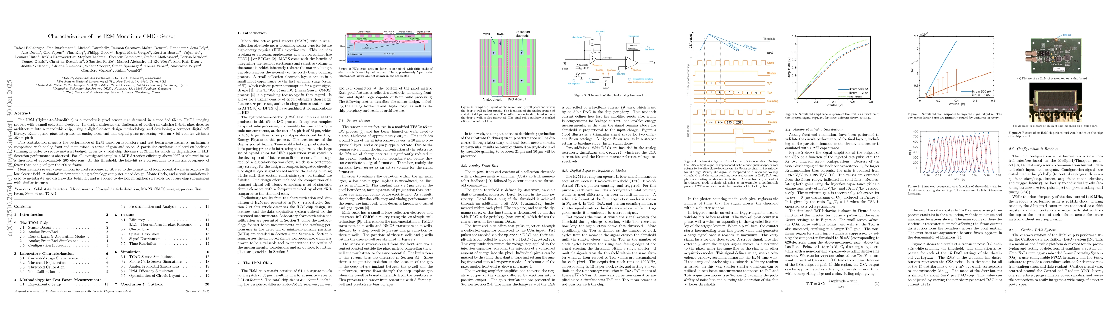
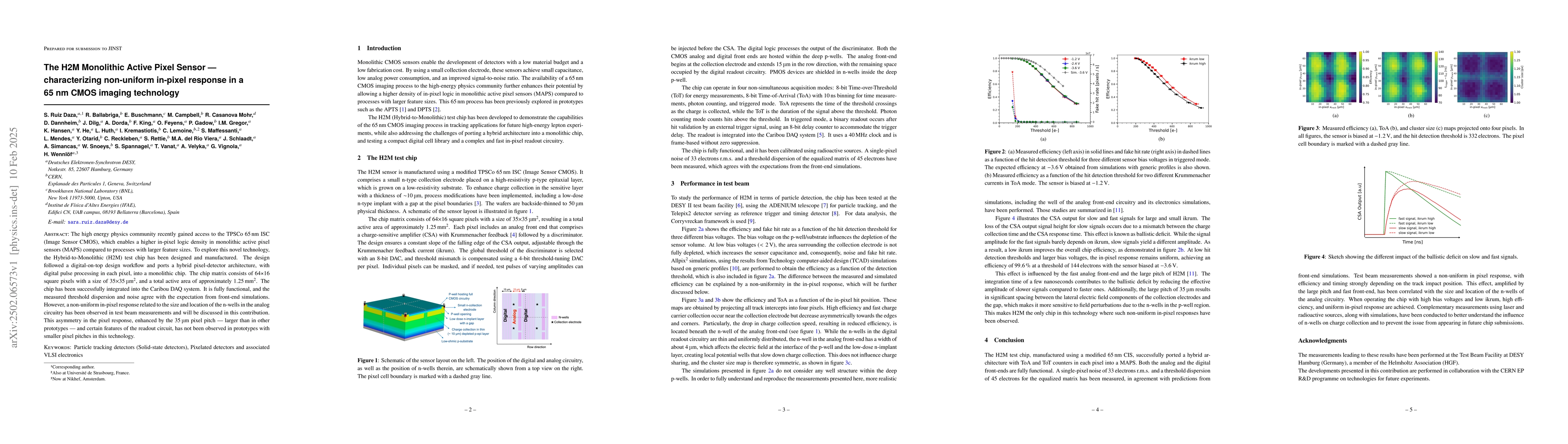
The H2M (Hybrid-to-Monolithic) is a monolithic pixel sensor manufactured in a modified \SI{65}{\nano\meter}~CMOS imaging process with a small collection electrode. Its design addresses the challenges ...

Thumbnail for High Density Hybridisation Using ENIG Bumping and Anisotropic Conductive Films

High Density Hybridisation Using ENIG Bumping and Anisotropic Conductive Films

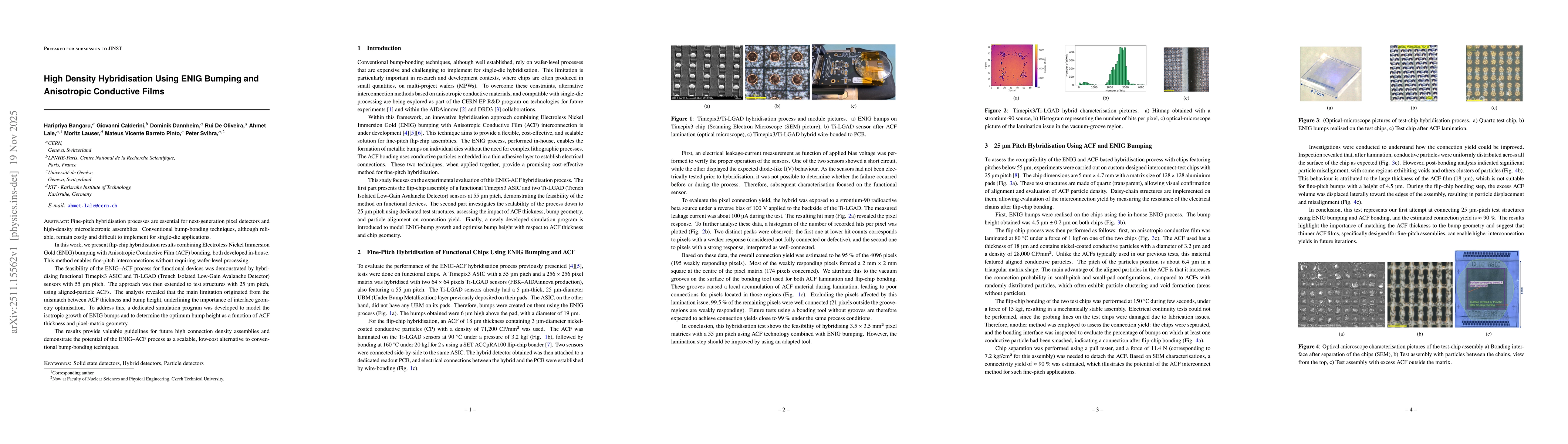
Fine-pitch hybridisation processes are essential for next-generation pixel detectors and high-density microelectronic assemblies. Conventional bump-bonding techniques, although reliable, remain costly...

Thumbnail for Advancements and future expansions of the Caribou DAQ system

Advancements and future expansions of the Caribou DAQ system

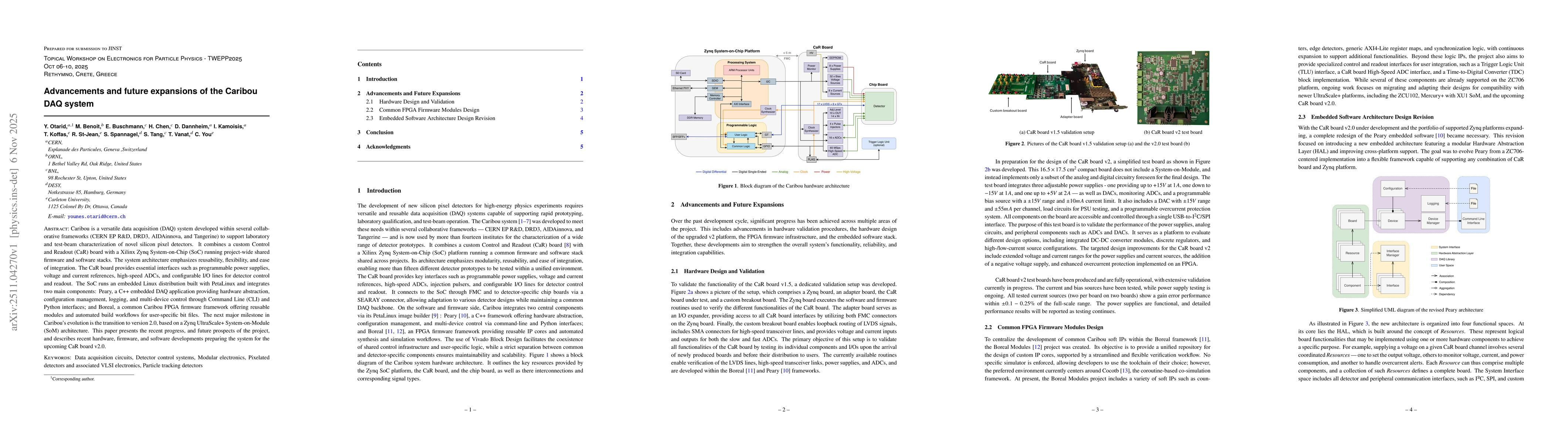
Caribou is a versatile data acquisition (DAQ) system developed within several collaborative frameworks (CERN EP R&D, DRD3, AIDAinnova, and Tangerine) to support laboratory and test-beam characterizati...

Thumbnail for Review of prototypes developed in a 65 nm CMOS imaging technology in view of vertexing applications at a future lepton collider

Review of prototypes developed in a 65 nm CMOS imaging technology in view of vertexing applications at a future lepton collider

The OCTOPUS project addresses the development and characterization of monolithic active pixel sensors in the TPSCo 65 nm ISC technology in view of vertexing applications at a future lepton collider. M...

This website uses cookies to ensure you get the best experience. Learn more