Academic Profile
Statistics
Similar Authors
Papers on arXiv
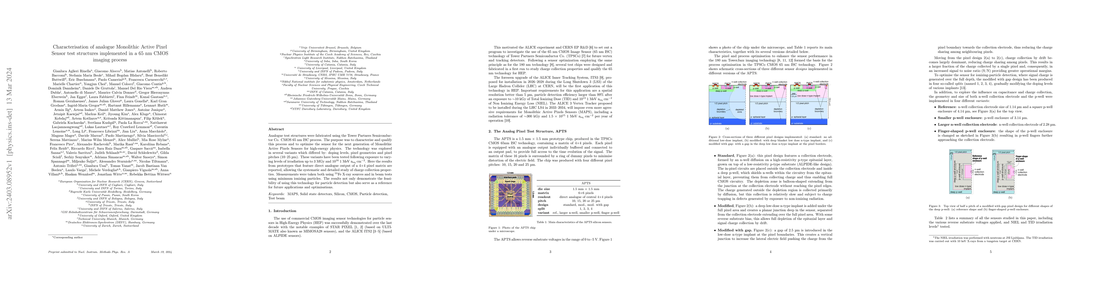
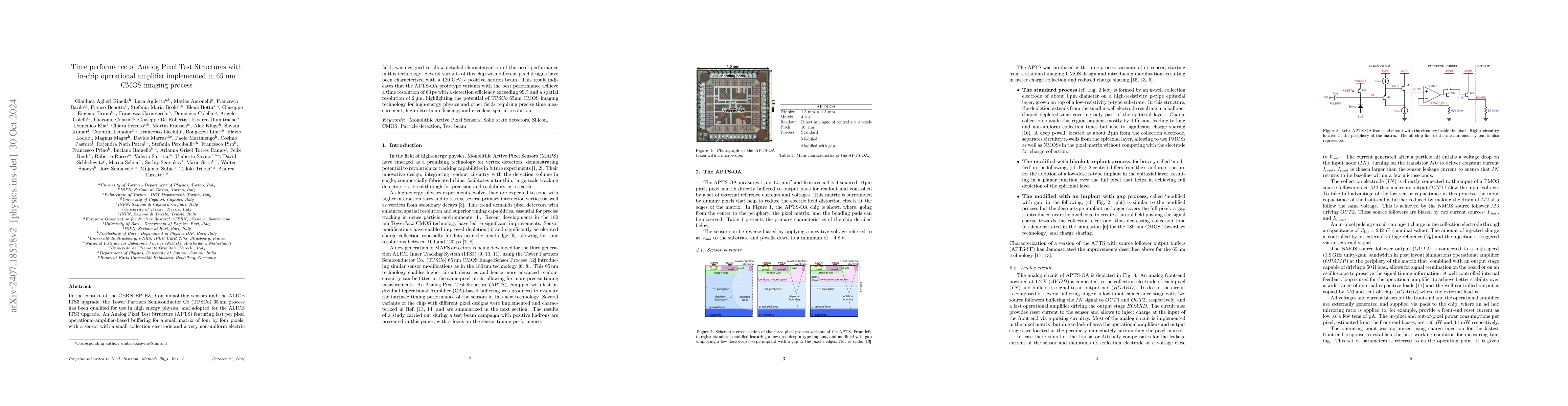
Analogue test structures were fabricated using the Tower Partners Semiconductor Co. CMOS 65 nm ISC process. The purpose was to characterise and qualify this process and to optimise the sensor for th...
Monolithic active pixel sensors (MAPS) produced in a 65 nm CMOS imaging technology are being investigated for applications in particle physics. The MAPS design has a small collection electrode chara...
Monolithic pixel detectors combine readout electronics and sensor in a single entity of silicon, which simplifies the production procedure and lowers the material budget compared to conventional hyb...
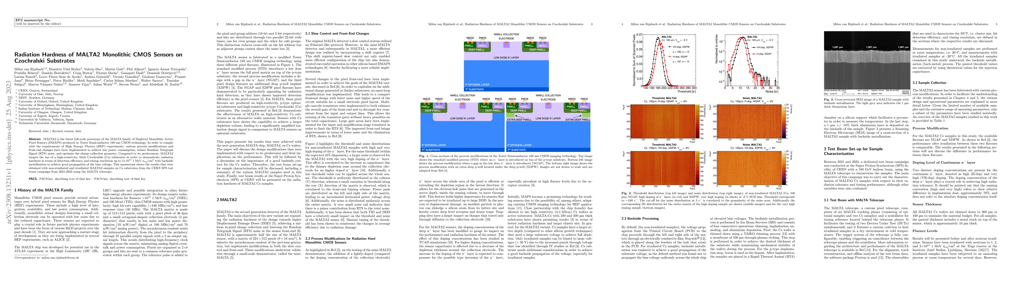
MALTA2 is the latest full-scale prototype of the MALTA family of Depleted Monolithic Active Pixel Sensors (DMAPS) produced in Tower Semiconductor 180 nm CMOS technology. In order to comply with the ...
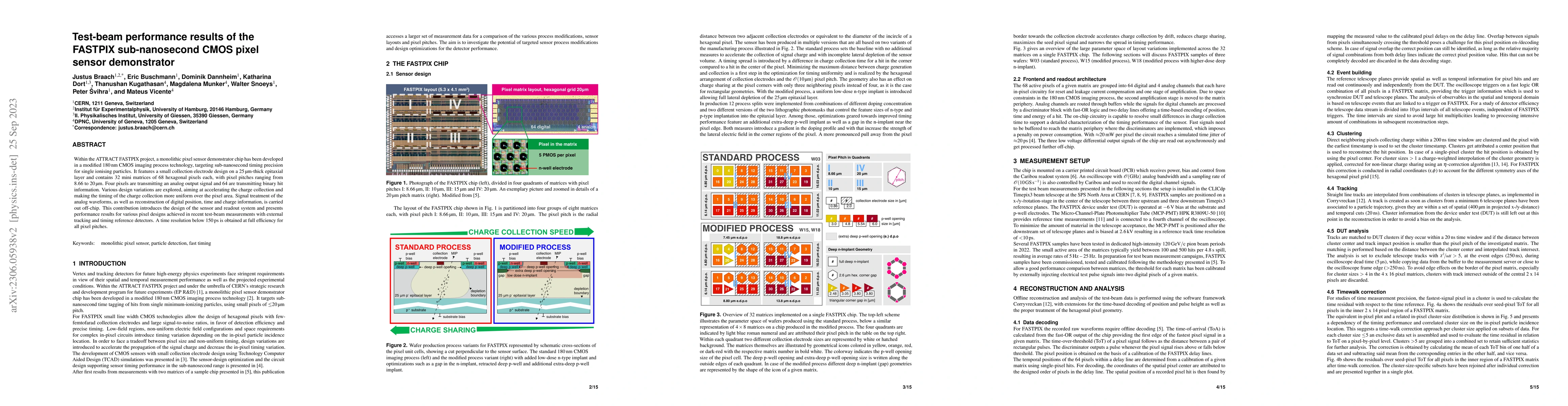
Within the ATTRACT FASTPIX project, a monolithic pixel sensor demonstrator chip has been developed in a modified 180 nm CMOS imaging process technology, targeting sub-nanosecond timing precision for...
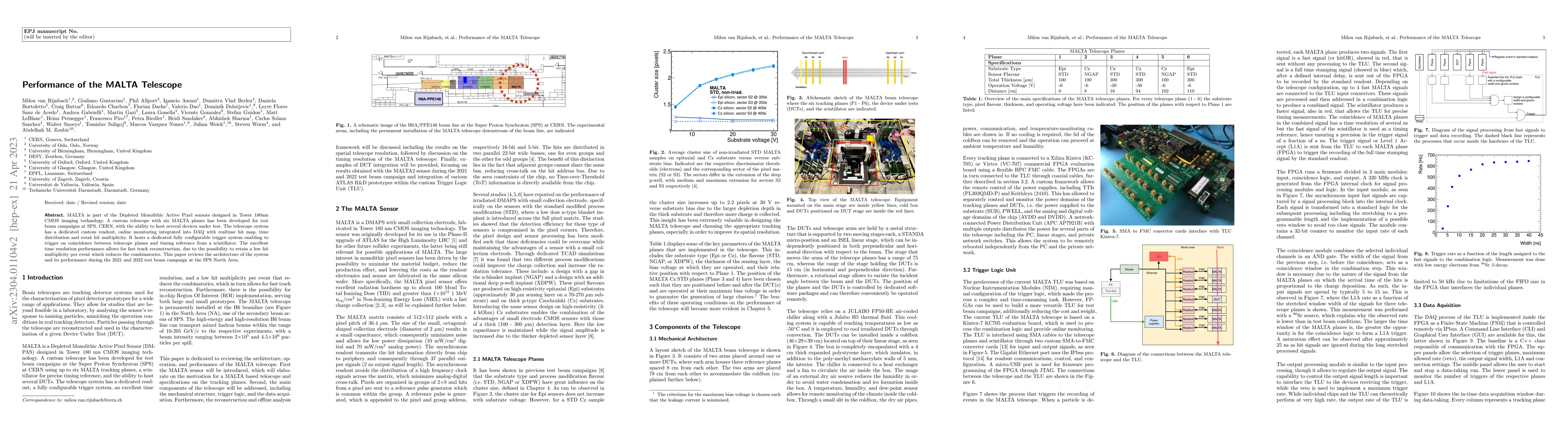
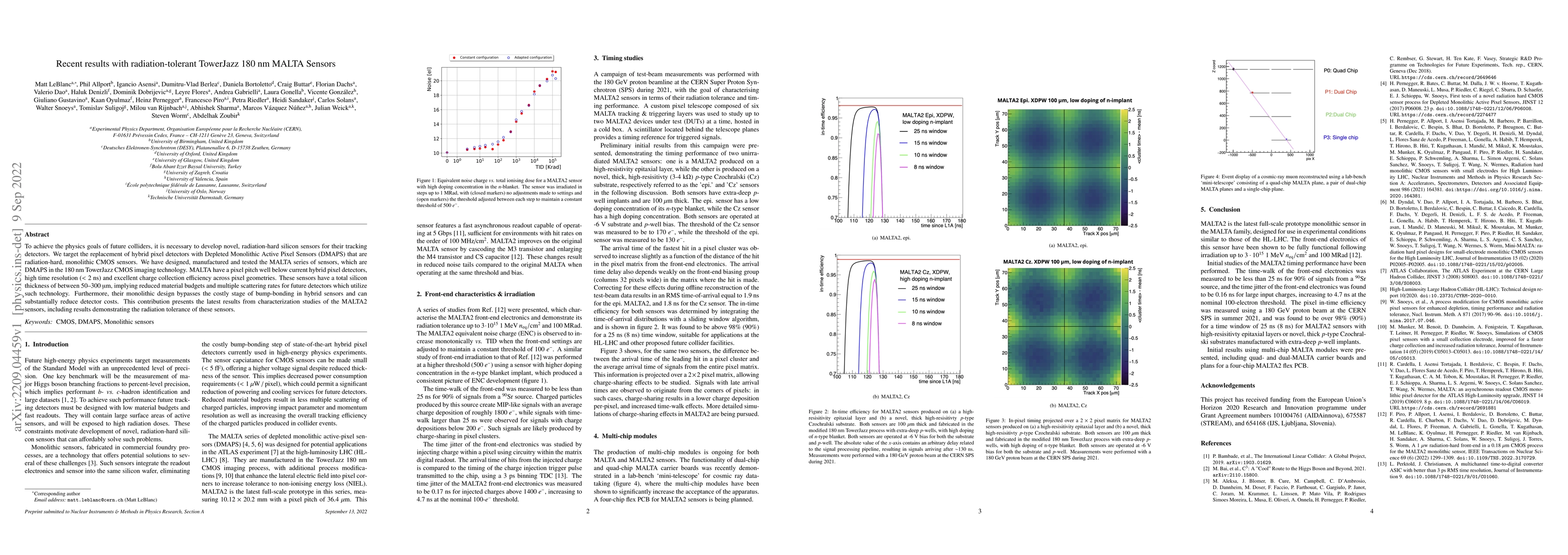
MALTA is part of the Depleted Monolithic Active Pixel sensors designed in Tower 180nm CMOS imaging technology. A custom telescope with six MALTA planes has been developed for test beam campaigns at ...
Monolithic CMOS sensors in a 65 nm imaging technology are being investigated by the CERN EP Strategic R&D Programme on Technologies for Future Experiments for an application in particle physics. The...
Monolithic CMOS pixel detectors have emerged as competitive contenders in the field of high-energy particle physics detectors. By utilizing commercial processes they offer high-volume production of ...
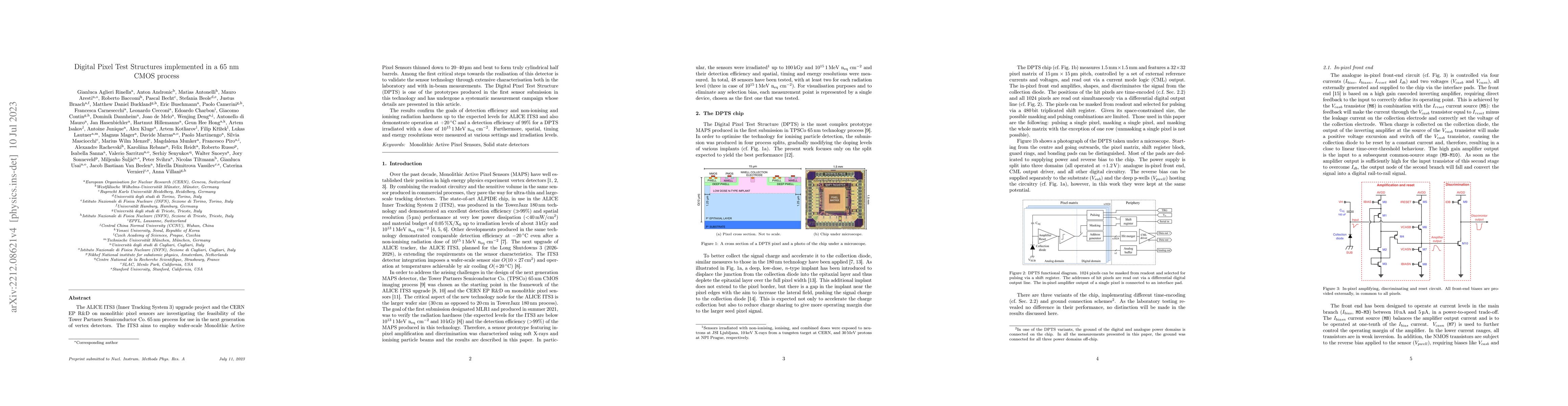
The ALICE ITS3 (Inner Tracking System 3) upgrade project and the CERN EP R&D on monolithic pixel sensors are investigating the feasibility of the Tower Partners Semiconductor Co. 65 nm process for u...
To achieve the physics goals of future colliders, it is necessary to develop novel, radiation-hard silicon sensors for their tracking detectors. We target the replacement of hybrid pixel detectors w...
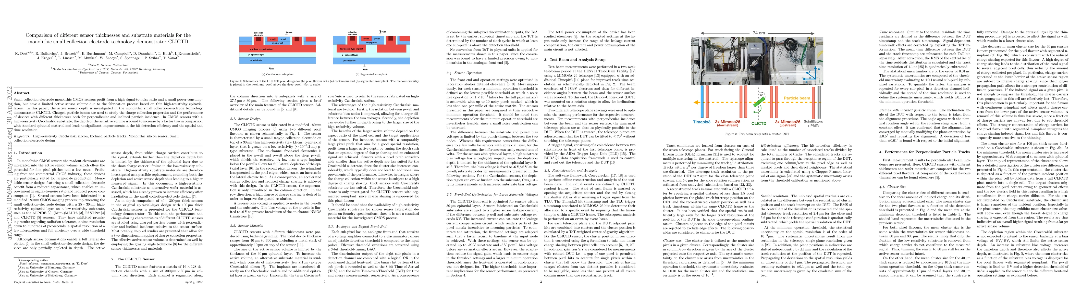
Small collection-electrode monolithic CMOS sensors profit from a high signal-to-noise ratio and a small power consumption, but have a limited active sensor volume due to the fabrication process base...
An ever-increasing demand for high-performance silicon sensors requires complex sensor designs that are challenging to simulate and model. The combination of electrostatic finite element simulations...
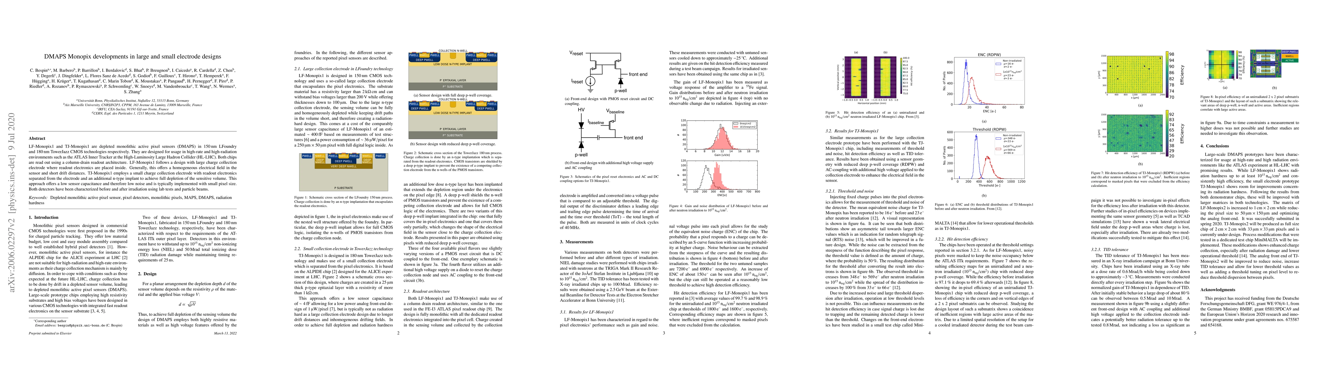
LF-Monopix1 and TJ-Monopix1 are depleted monolithic active pixel sensors (DMAPS) in 150 nm LFoundry and 180 nm TowerJazz CMOS technologies respectively. They are designed for usage in high-rate and ...
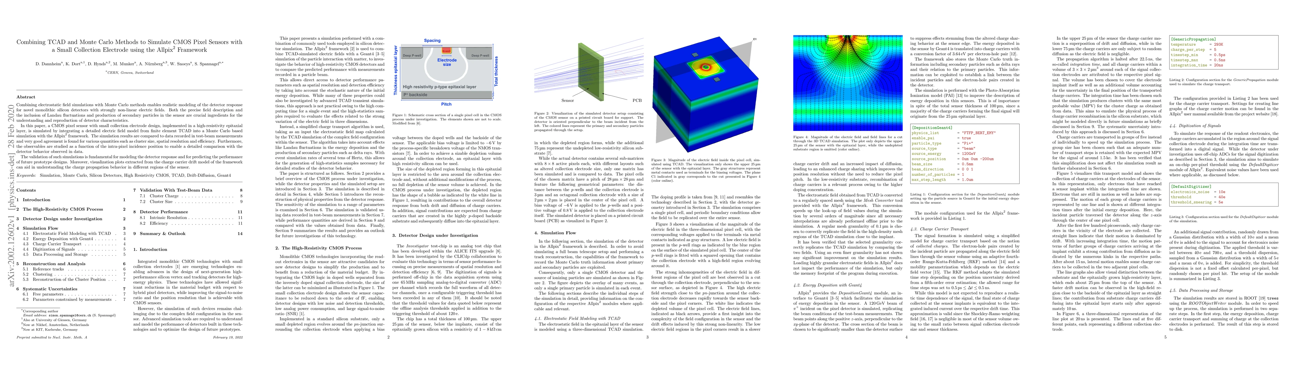
Combining electrostatic field simulations with Monte Carlo methods enables realistic modeling of the detector response for novel monolithic silicon detectors with strongly non-linear electric fields...
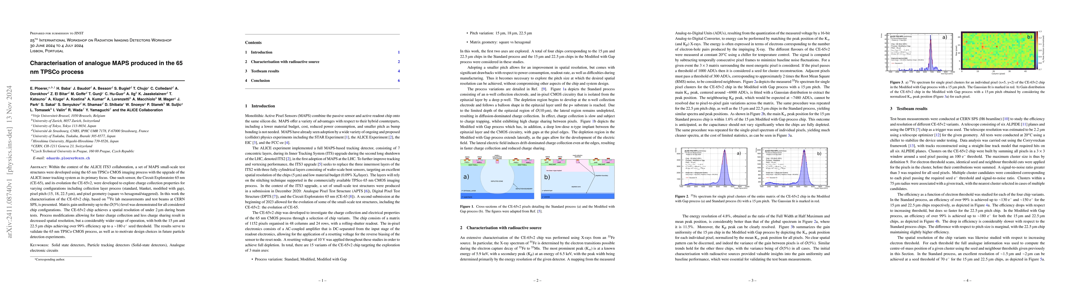
Within the context of the ALICE ITS3 collaboration, a set of MAPS small-scale test structures were developed using the 65 nm TPSCo CMOS imaging process with the upgrade of the ALICE inner tracking sys...
In the context of the CERN EP R&D on monolithic sensors and the ALICE ITS3 upgrade, the Tower Partners Semiconductor Co (TPSCo) 65 nm process has been qualified for use in high energy physics, and ado...
The optimisation of the sensitive region of CMOS sensors with complex non-uniform electric fields requires precise simulations, and this can be achieved by a combination of electrostatic field simulat...
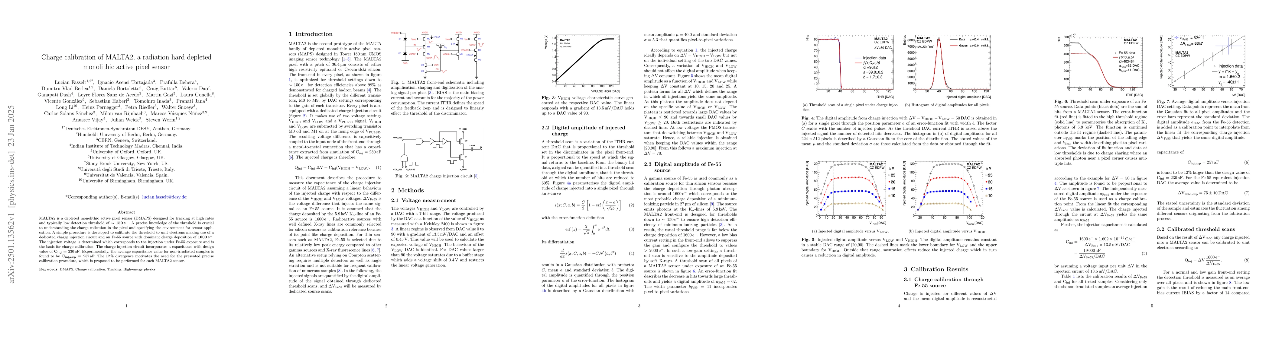
MALTA2 is a depleted monolithic active pixel sensor (DMAPS) designed for tracking at high rates and typically low detection threshold of $\sim150\,\mathrm{e^-}$. A precise knowledge of the threshold i...
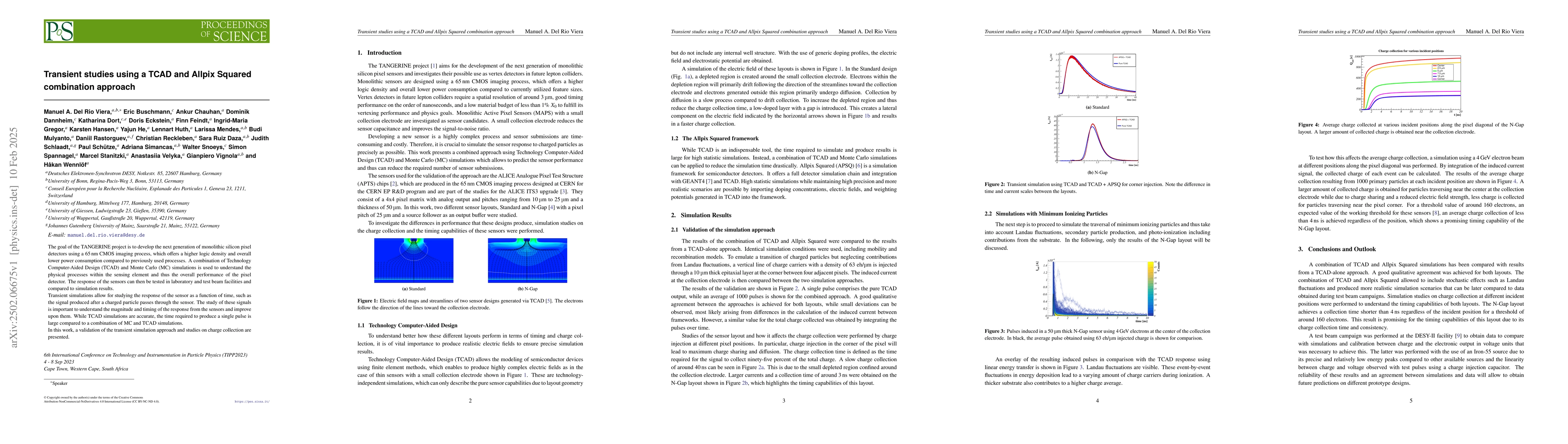
The goal of the TANGERINE project is to develop the next generation of monolithic silicon pixel detectors using a 65 nm CMOS imaging process, which offers a higher logic density and overall lower powe...
The high energy physics community recently gained access to the TPSCo 65 nm ISC (Image Sensor CMOS), which enables a higher in-pixel logic density in monolithic active pixel sensors (MAPS) compared to...
CERN's strategic R&D programme on technologies for future experiments recently started investigating the TPSCo 65nm ISC CMOS imaging process for monolithic active pixels sensors for application in hig...
The next generation of MAPS for future tracking detectors will have to meet stringent requirements placed on them. One such detector is the ALICE ITS3 that aims to be very light at 0.07% X/X$_{0}$ per...
Monolithic active pixel sensors with depleted substrates present a promising option for pixel detectors in high-radiation environments. High-resistivity silicon substrates and high bias voltage capabi...
In the LHC long shutdown 3, the ALICE experiment upgrades the inner layers of its Inner Tracker System with three layers of wafer-scale stitched sensors bent around the beam pipe. Two stitched sensor ...
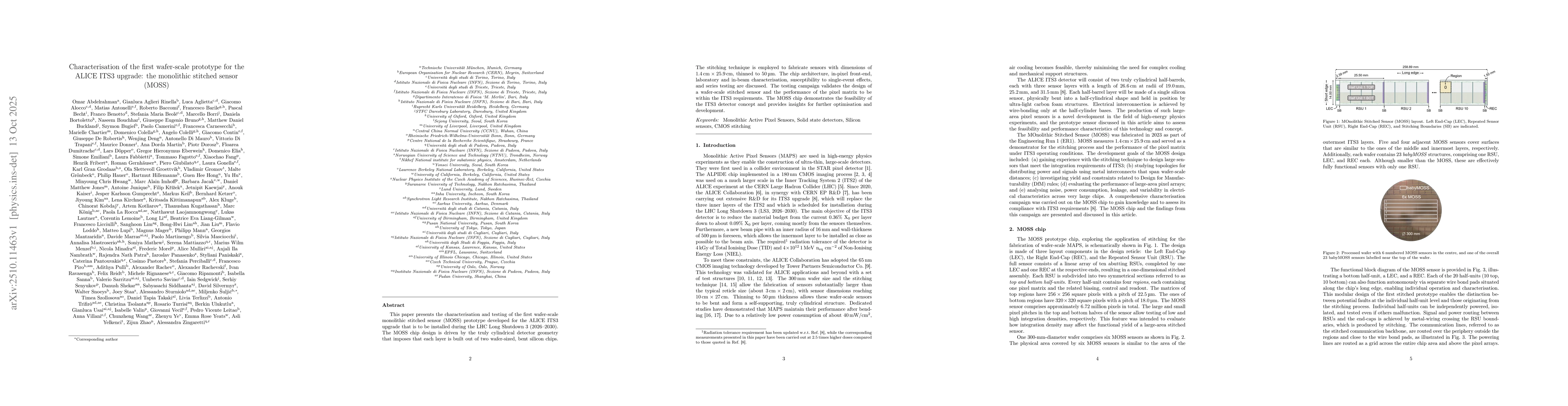
This paper presents the characterisation and testing of the first wafer-scale monolithic stitched sensor (MOSS) prototype developed for the ALICE ITS3 upgrade that is to be installed during the LHC Lo...
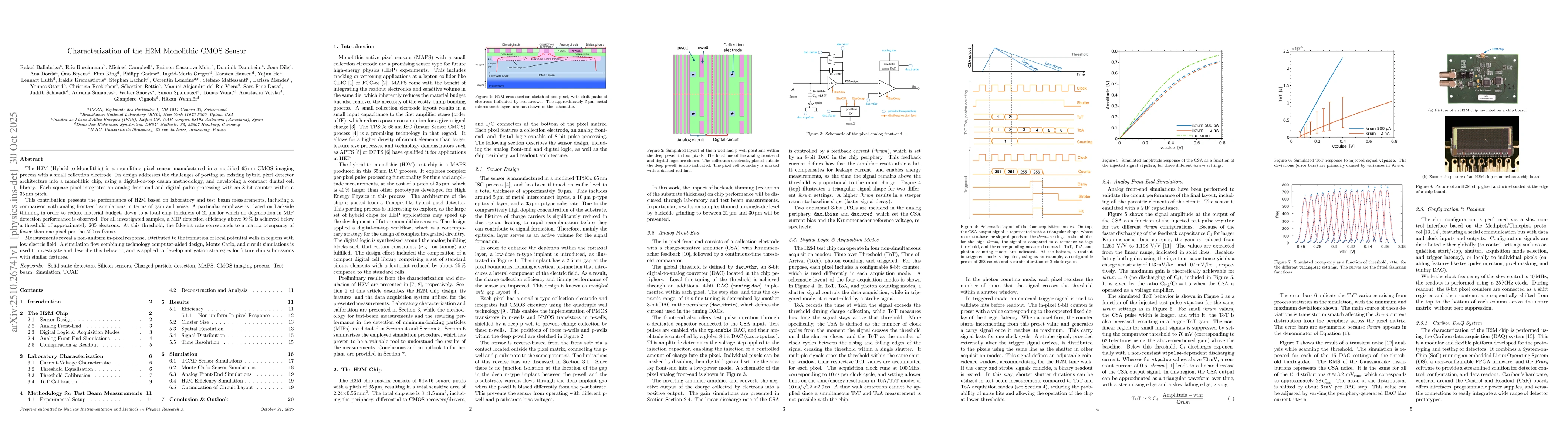
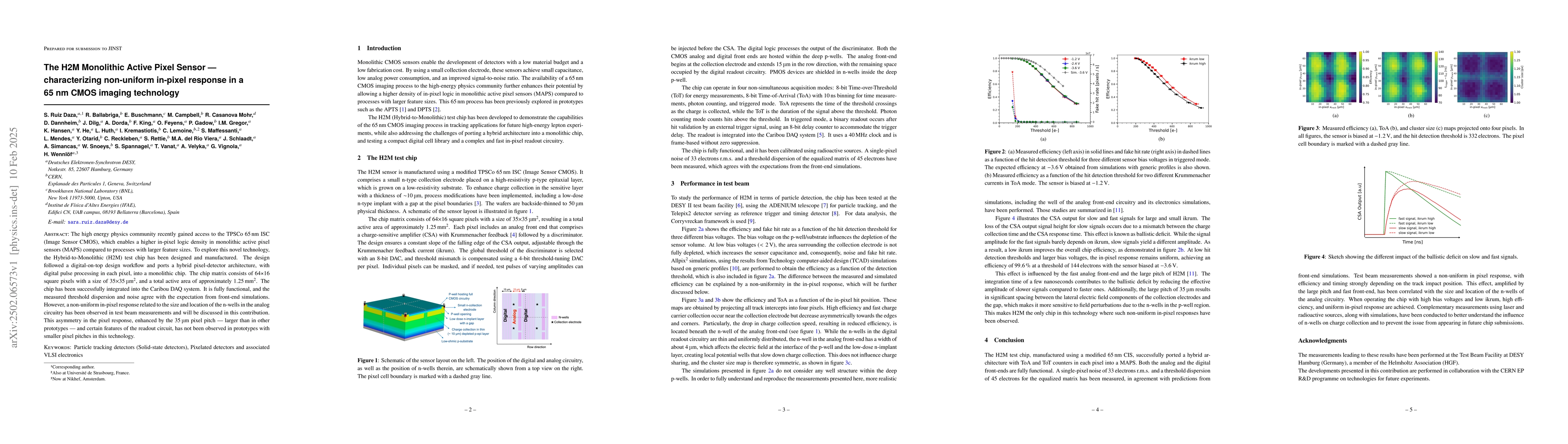
The H2M (Hybrid-to-Monolithic) is a monolithic pixel sensor manufactured in a modified \SI{65}{\nano\meter}~CMOS imaging process with a small collection electrode. Its design addresses the challenges ...
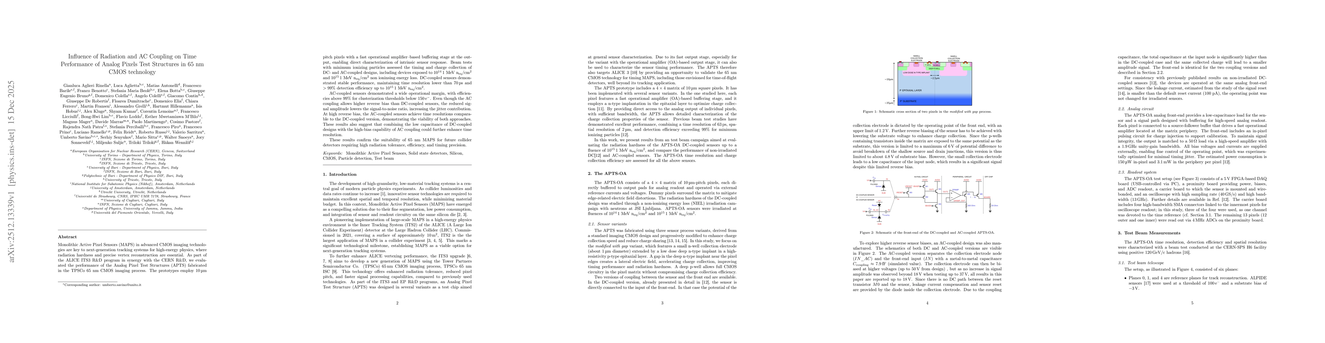
Monolithic Active Pixel Sensors (MAPS) in advanced CMOS imaging technologies are key to next-generation tracking systems for high-energy physics, where radiation hardness and precise vertex reconstruc...
For the Inner Tracking System 3 (ITS3) upgrade, the ALICE experiment at CERN requires monolithic active pixel sensors of dimensions up to 97~mm$\,\times\,$266~mm, occupying a large fraction of a 300 m...
A parametric simulation tool for pixel sensors is presented. A realistic pixel response is simulated purely based on measurement input, without requiring detailed knowledge of the underlying manufactu...