ArxivLens
G
Researcher

Gianluca Aglieri Rinella

9 papers on arXiv

9 arXiv Papers
275 Total Publications
Profile

Academic Profile

Name G. Aglieri Rinella
Total Papers 275
Scholar Profile View on Semantic Scholar
Metrics

Statistics

9 arXiv Papers
275 Total Publications
Publications

Papers on arXiv

Thumbnail for Characterisation of analogue Monolithic Active Pixel Sensor test
  structures implemented in a 65 nm CMOS imaging process
arXiv
Characterisation of analogue Monolithic Active Pixel Sensor test structures implemented in a 65 nm CMOS imaging process

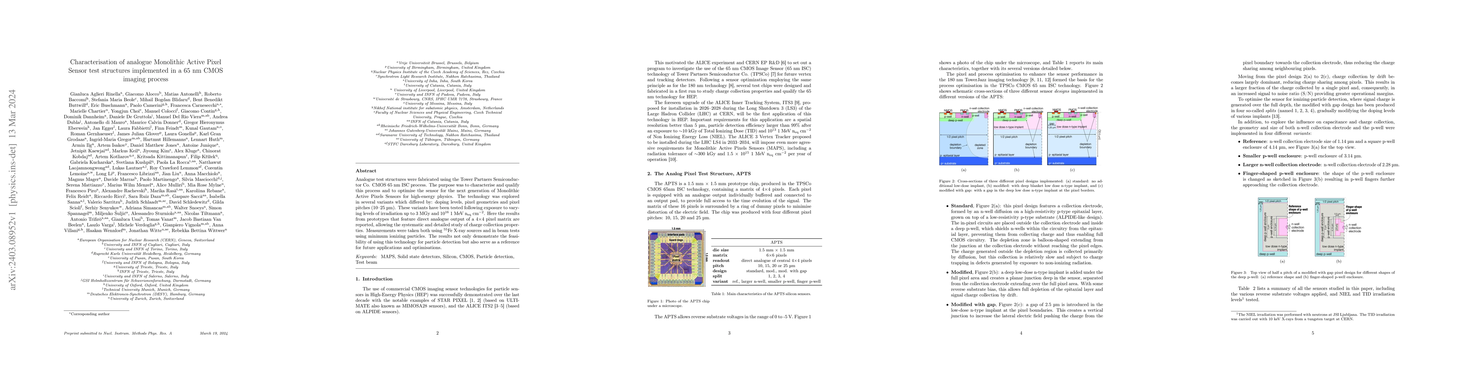
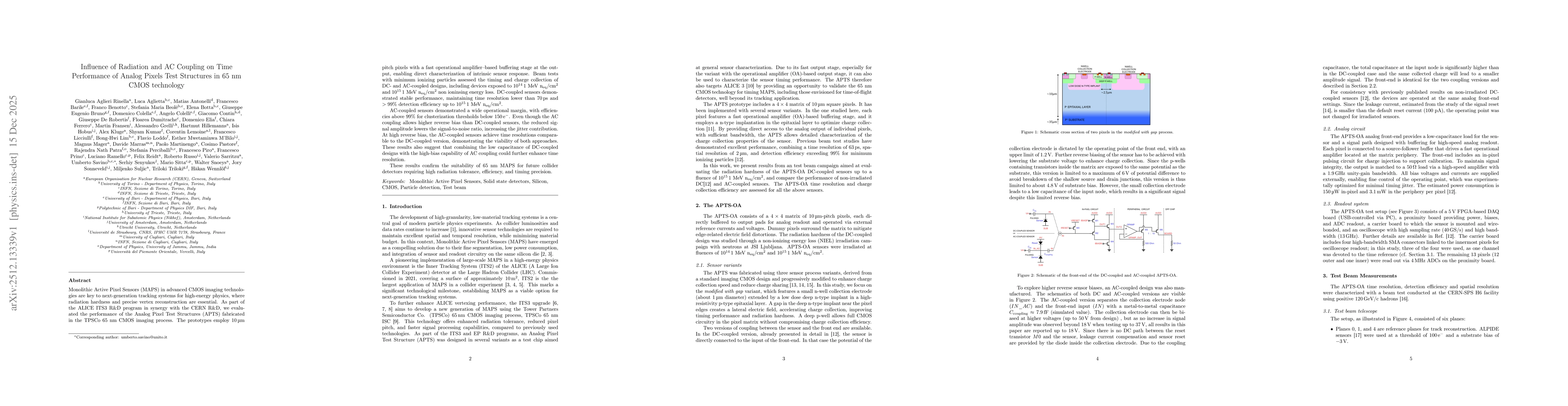
Analogue test structures were fabricated using the Tower Partners Semiconductor Co. CMOS 65 nm ISC process. The purpose was to characterise and qualify this process and to optimise the sensor for th...

Thumbnail for Digital Pixel Test Structures implemented in a 65 nm CMOS process
arXiv
Digital Pixel Test Structures implemented in a 65 nm CMOS process

The ALICE ITS3 (Inner Tracking System 3) upgrade project and the CERN EP R&D on monolithic pixel sensors are investigating the feasibility of the Tower Partners Semiconductor Co. 65 nm process for u...

Thumbnail for Remote Configuration of the ProASIC3 on the ALICE Inner Tracking System
  Readout Unit
arXiv
Remote Configuration of the ProASIC3 on the ALICE Inner Tracking System Readout Unit

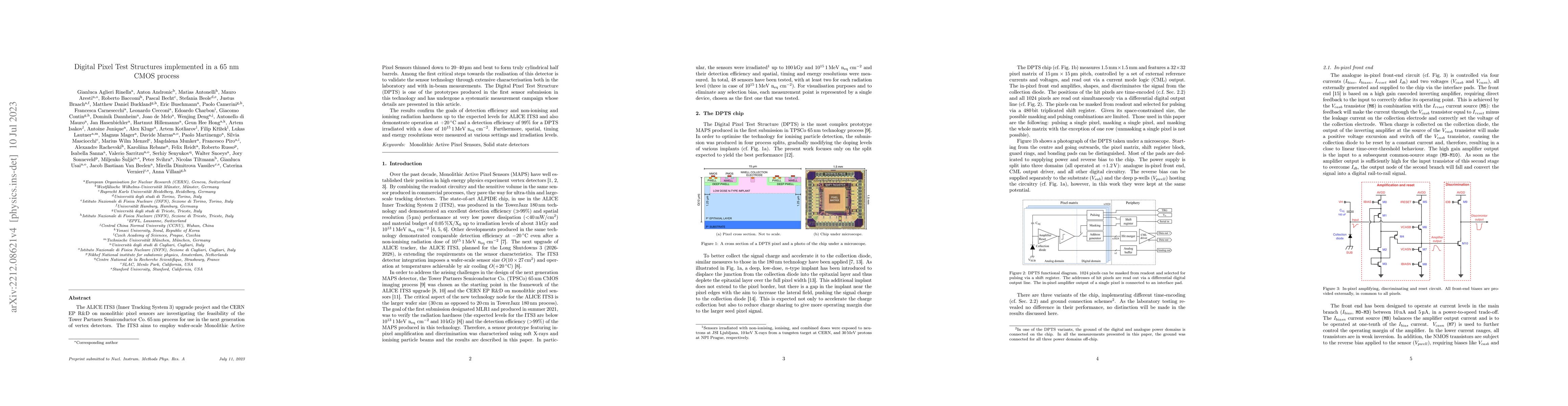
A Large Ion Collider Experiment (ALICE) is one of the four major experiments conducted at the CERN Large Hadron Collider (LHC). The ALICE detector is currently undergoing an upgrade for the upcoming...

Thumbnail for Time resolution of silicon pixel sensors
arXiv
Time resolution of silicon pixel sensors

We derive expressions for the time resolution of silicon detectors, using the Landau theory and a PAI model for describing the charge deposit of high energy particles. First we use the centroid time...

Thumbnail for Time performance of Analog Pixel Test Structures with in-chip
  operational amplifier implemented in 65 nm CMOS imaging process
arXiv
Time performance of Analog Pixel Test Structures with in-chip operational amplifier implemented in 65 nm CMOS imaging process

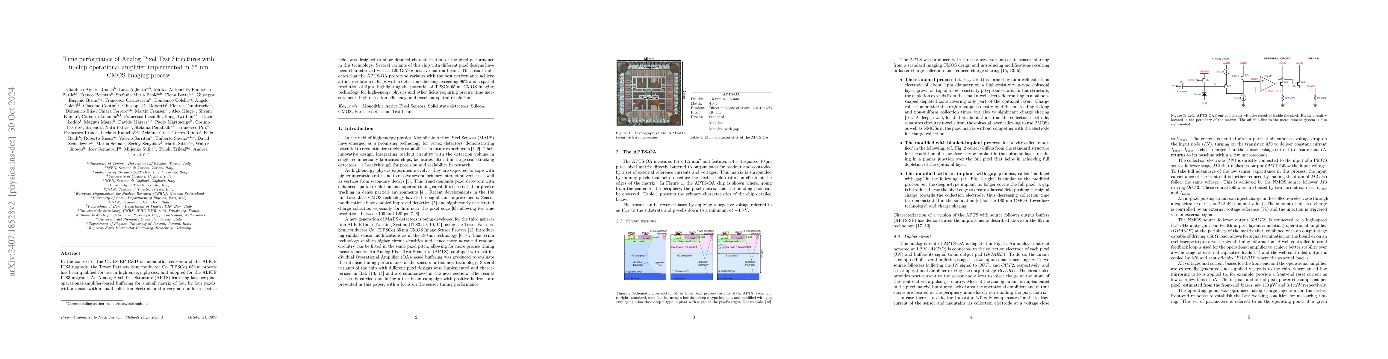
In the context of the CERN EP R&D on monolithic sensors and the ALICE ITS3 upgrade, the Tower Partners Semiconductor Co (TPSCo) 65 nm process has been qualified for use in high energy physics, and ado...

Thumbnail for Further Characterisation of Digital Pixel Test Structures Implemented in
  a 65 nm CMOS Process
arXiv
Further Characterisation of Digital Pixel Test Structures Implemented in a 65 nm CMOS Process

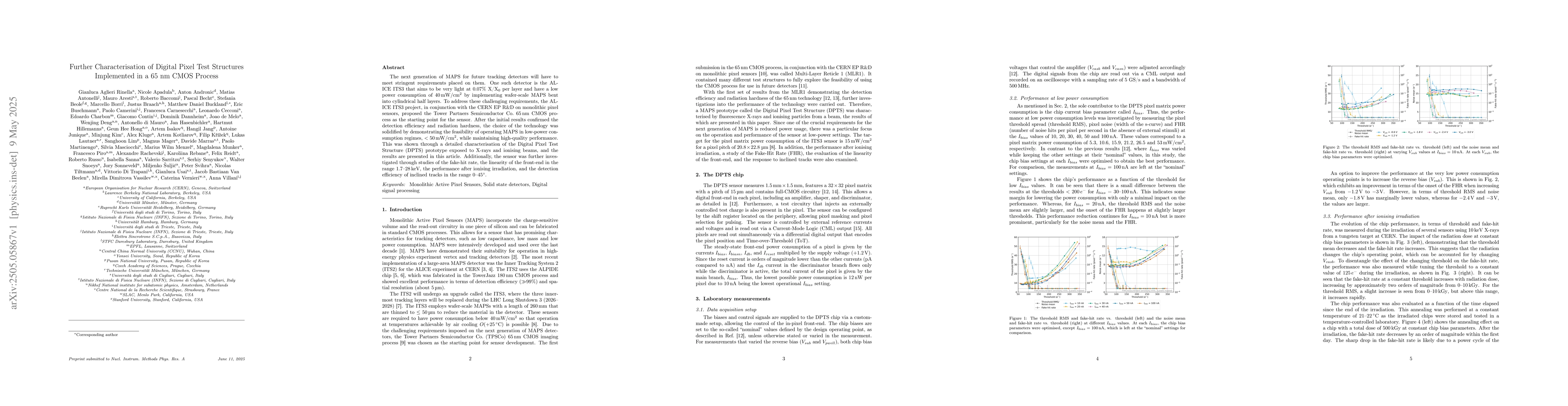
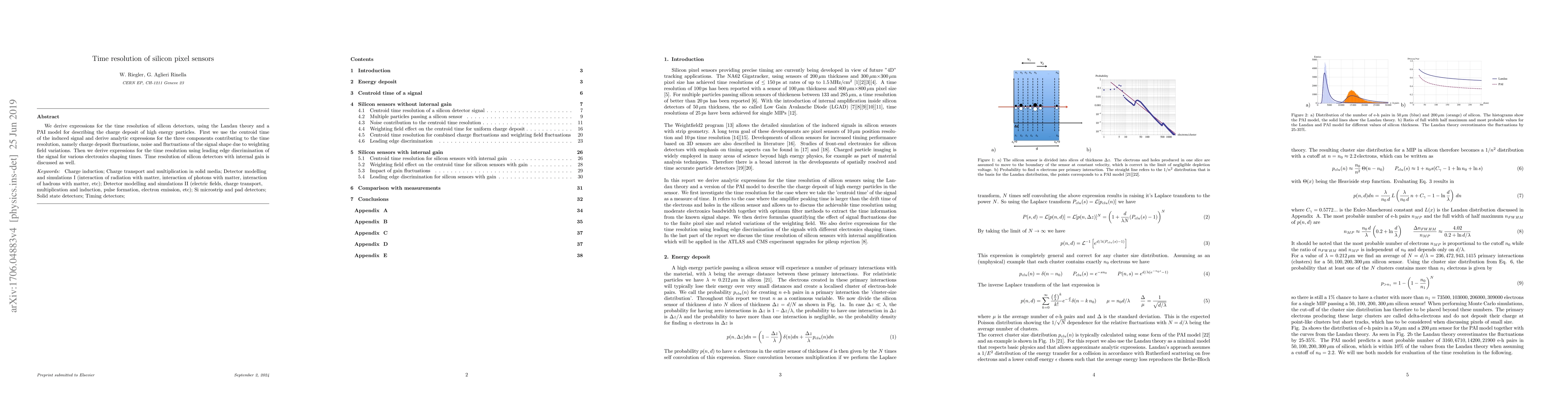
The next generation of MAPS for future tracking detectors will have to meet stringent requirements placed on them. One such detector is the ALICE ITS3 that aims to be very light at 0.07% X/X$_{0}$ per...

Thumbnail for Characterisation of the first wafer-scale prototype for the ALICE ITS3
  upgrade: the monolithic stitched sensor (MOSS)
arXiv
Characterisation of the first wafer-scale prototype for the ALICE ITS3 upgrade: the monolithic stitched sensor (MOSS)

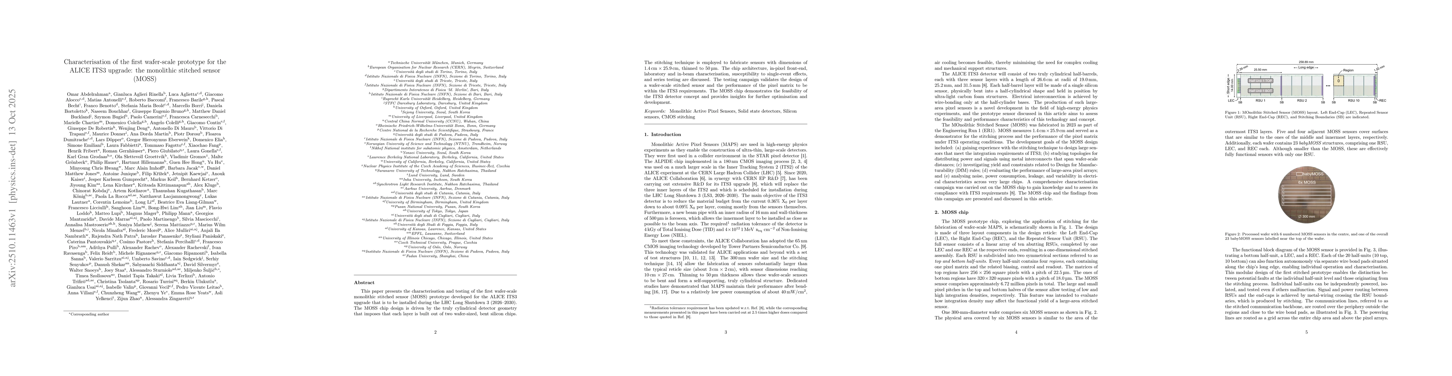
This paper presents the characterisation and testing of the first wafer-scale monolithic stitched sensor (MOSS) prototype developed for the ALICE ITS3 upgrade that is to be installed during the LHC Lo...

Thumbnail for Influence of Radiation and AC Coupling on Time Performance of Analog Pixels Test Structures in 65 nm CMOS technology
arXiv
Influence of Radiation and AC Coupling on Time Performance of Analog Pixels Test Structures in 65 nm CMOS technology

Monolithic Active Pixel Sensors (MAPS) in advanced CMOS imaging technologies are key to next-generation tracking systems for high-energy physics, where radiation hardness and precise vertex reconstruc...

Thumbnail for A Novel Approach for Fault Detection and Failure Analysis of CMOS Copper Metal Stacks
arXiv
A Novel Approach for Fault Detection and Failure Analysis of CMOS Copper Metal Stacks

For the Inner Tracking System 3 (ITS3) upgrade, the ALICE experiment at CERN requires monolithic active pixel sensors of dimensions up to 97~mm$\,\times\,$266~mm, occupying a large fraction of a 300 m...

This website uses cookies to ensure you get the best experience. Learn more