Academic Profile
Statistics
Similar Authors
Papers on arXiv
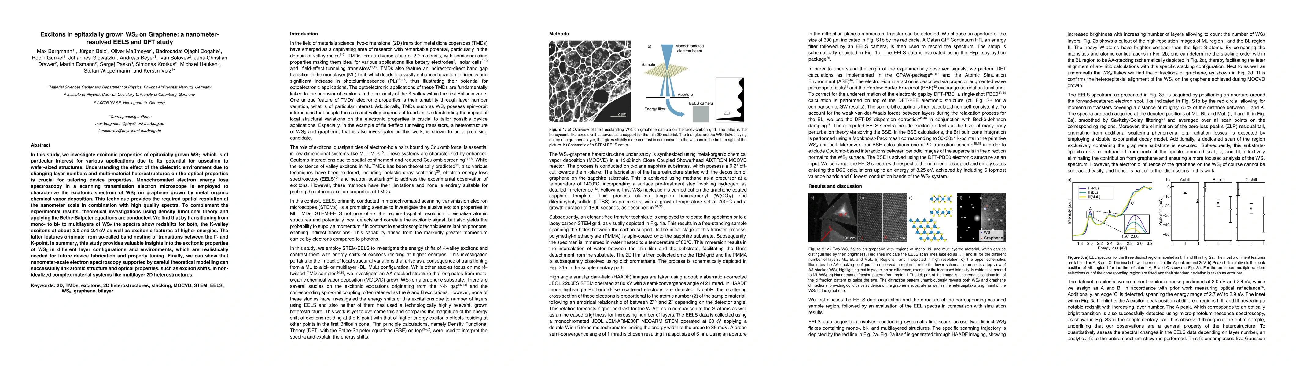
In this study, we investigate excitonic properties of epitaxially grown WS2, which is of particular interest for various applications due to its potential for upscaling to wafer sized structures. Un...
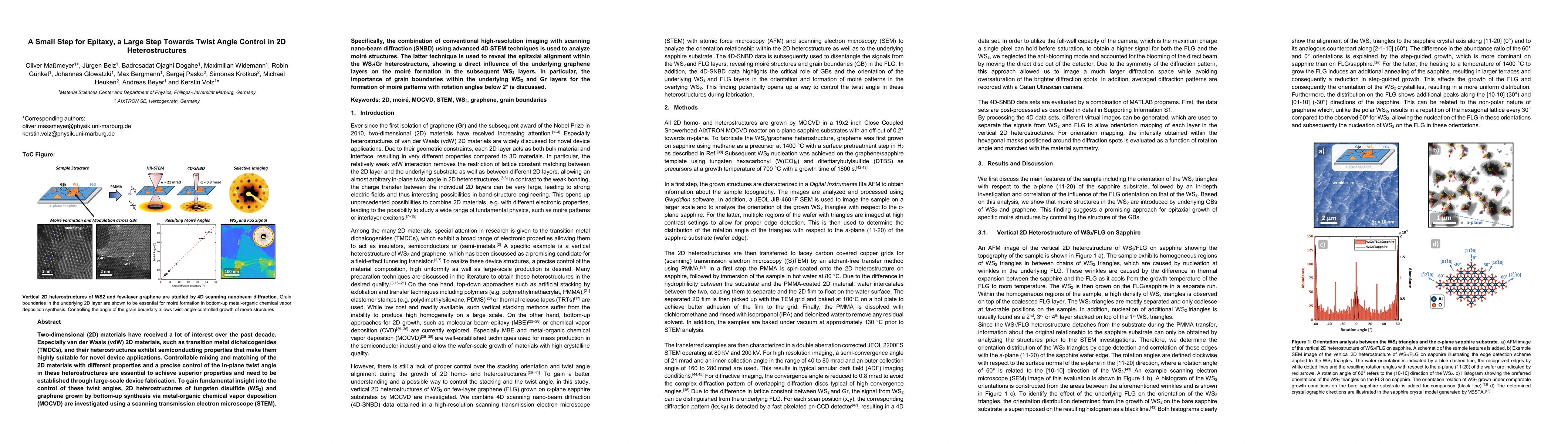
Two-dimensional (2D) materials have received a lot of interest over the past decade. Especially van der Waals (vdW) 2D materials, such as transition metal dichalcogenides (TMDCs), and their heterost...
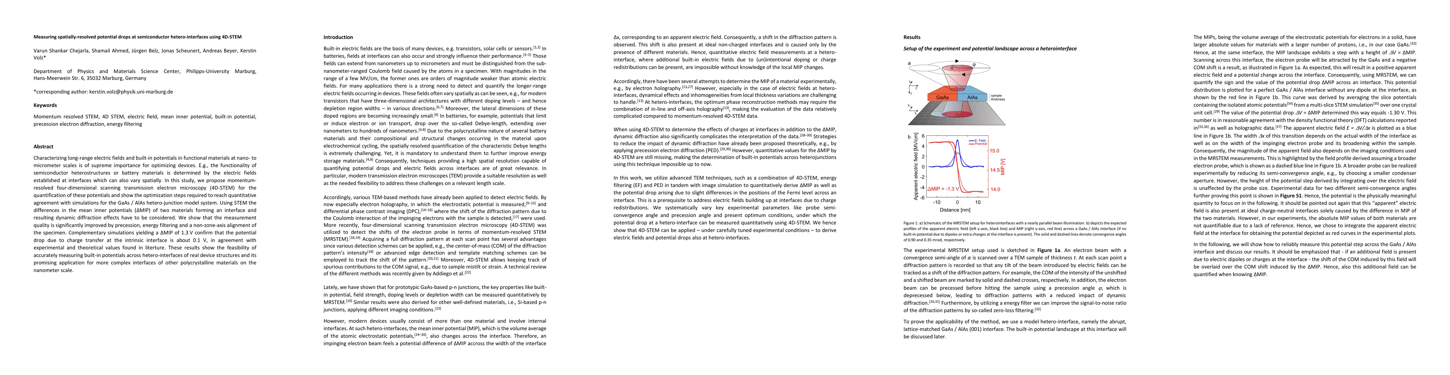
Characterizing long-range electric fields and built-in potentials in functional materials at nano- to micrometer scales is of supreme importance for optimizing devices. E.g., the functionality of se...
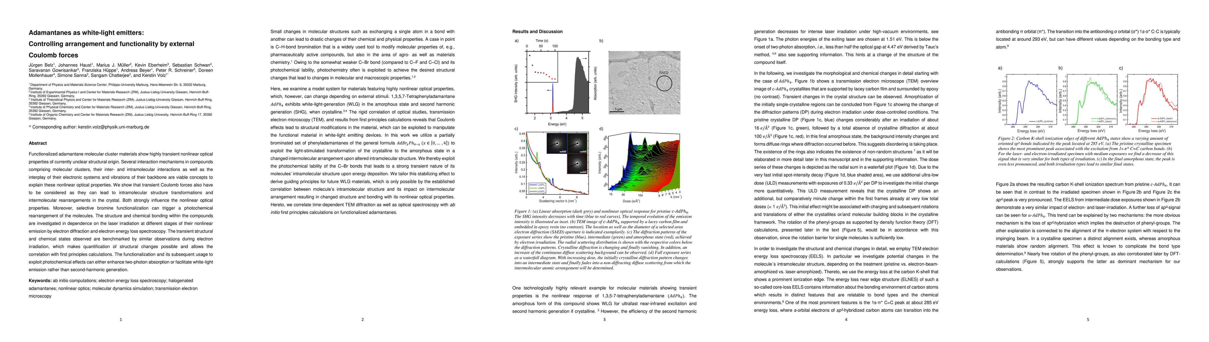
Functionalized adamantane molecular cluster materials show highly transient nonlinear optical properties of currently unclear structural origin. Several interaction mechanisms in compounds comprisin...
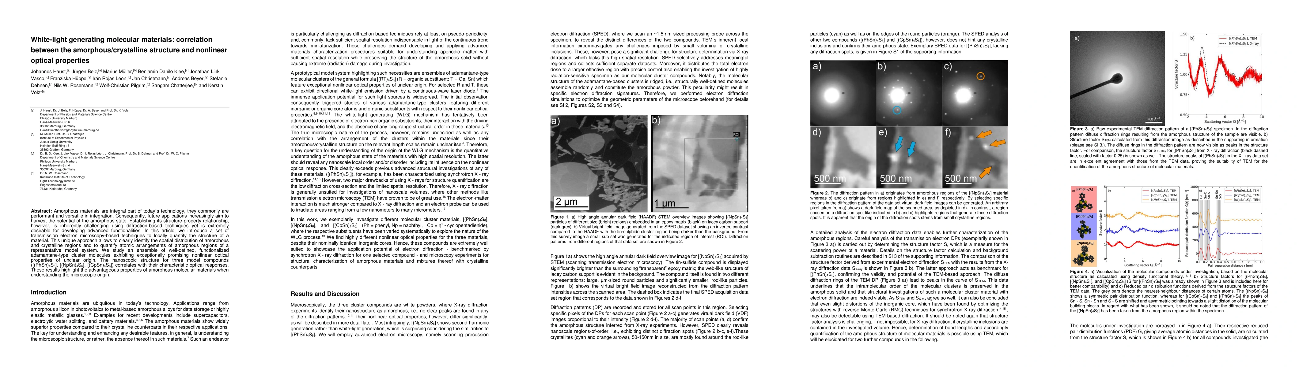
Amorphous materials are integral part of todays technology, they commonly are performant and versatile in integration. Consequently, future applications increasingly aim to harvest the potential of ...
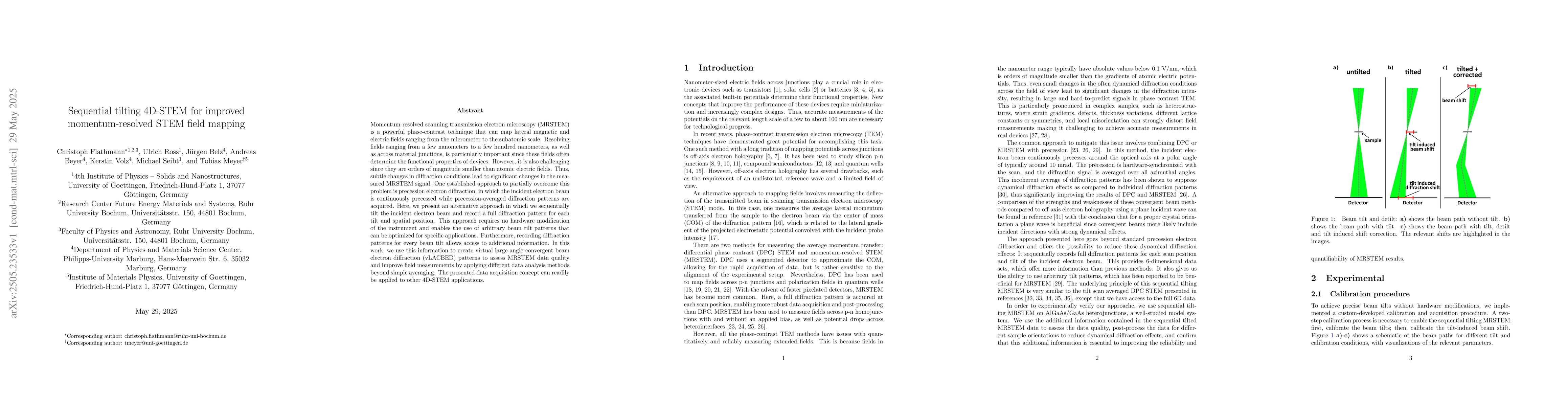
Momentum-resolved scanning transmission electron microscopy (MRSTEM) is a powerful phase-contrast technique that can map lateral magnetic and electric fields ranging from the micrometer to the subatom...
Polycrystalline materials have numerous applications due to their unique properties, which are often determined by the grain boundaries. Hence, quantitative characterization of grain as well as interf...
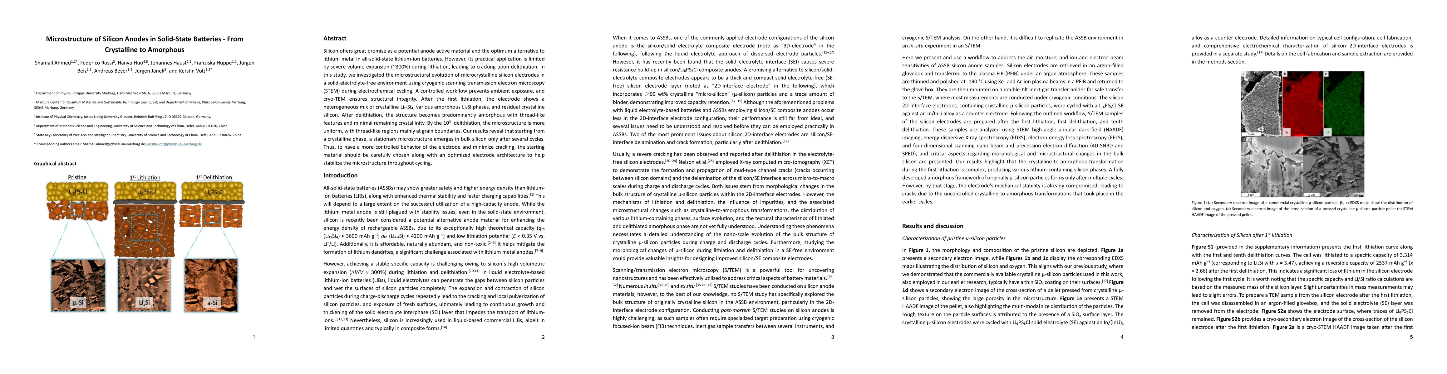
Silicon offers great promise as a potential anode active material and the optimum alternative to lithium metal in all-solid-state lithium-ion batteries. However, its practical application is limited b...
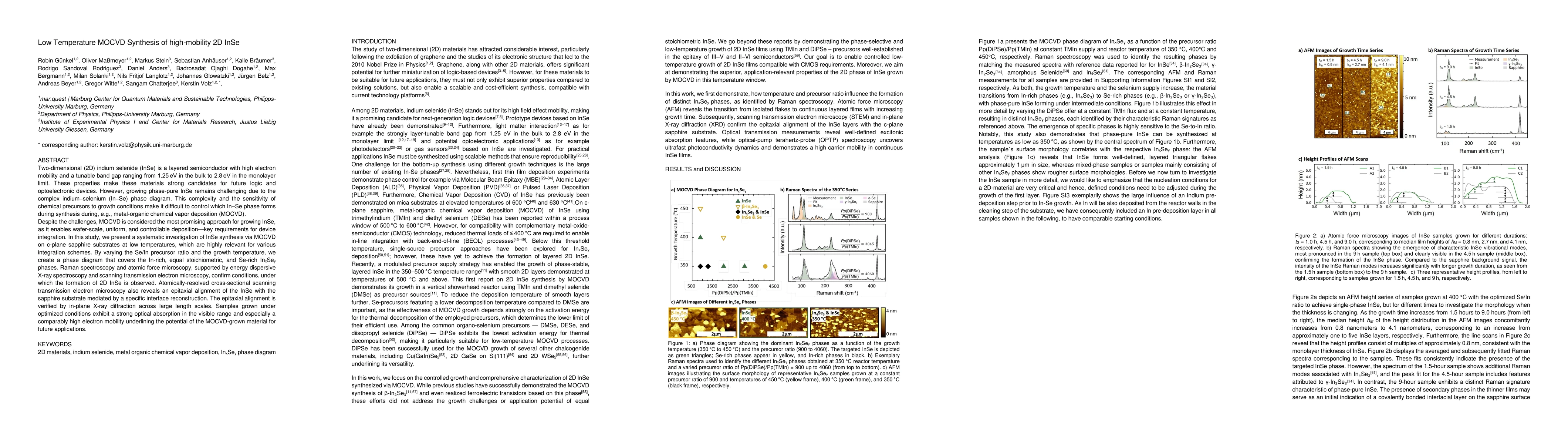
Two-dimensional (2D) indium selenide (InSe) is a layered semiconductor with high electron mobility and a tunable band gap ranging from 1.25 eV in the bulk to 2.8 eV in the monolayer limit. These prope...
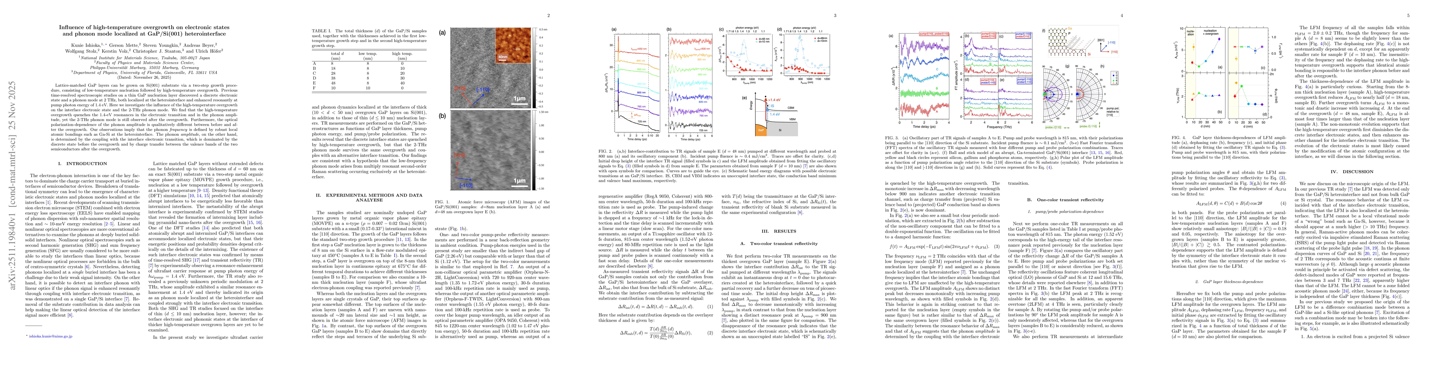
Lattice-matched GaP layers can be grown on Si(001) substrate via a two-step growth procedure, consisting of low-temperature nucleation followed by high-temperature overgrowth. Previous time-resolved s...

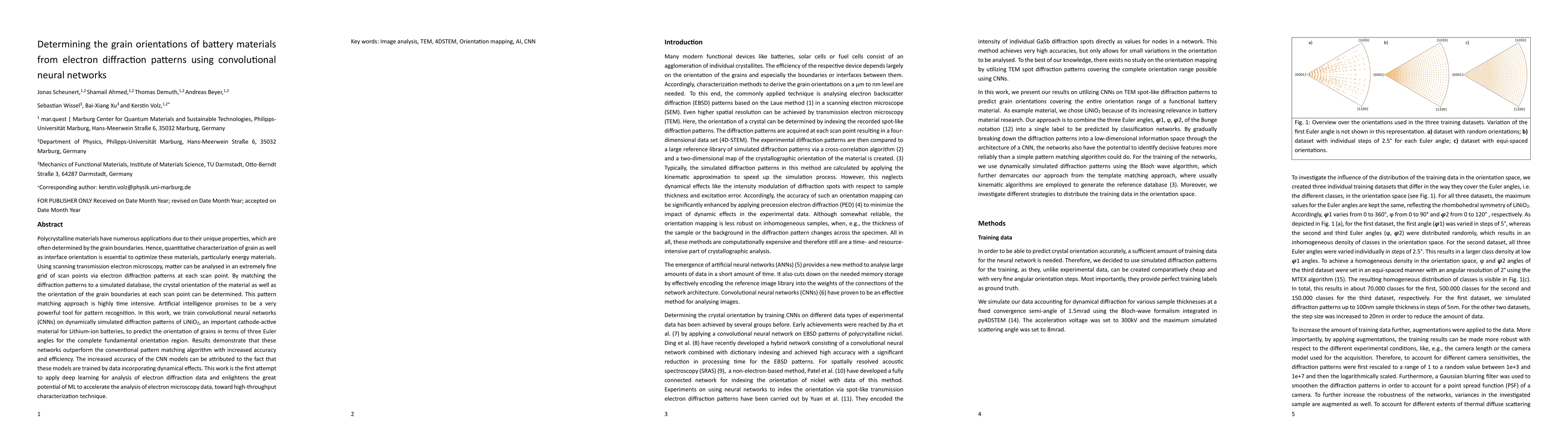
The properties of polycrystalline materials are strongly influenced by the spatial arrangement and orientations of individual grains within the microstructure, making nanoscale characterization of gra...