01
MethodologyHow they did it
Brief description of the research methodology used
This study utilizes 4D-STEM to quantify spatially-resolved potential drops at semiconductor hetero-interfaces, employing optimization techniques like precession and energy filtering. Results show a potential drop of 0.1 V at the GaAs/AlAs interface, validating the method's accuracy for characterizing built-in potentials in device structures.
This study utilizes 4D-STEM to quantify spatially-resolved potential drops at semiconductor hetero-interfaces, employing optimization techniques like precession and energy filtering. Results show a potential drop of 0.1 V at the GaAs/AlAs interface, validating the method's accuracy for characterizing built-in potentials in device structures.
Brief description of the research methodology used More in Methodology →
Main finding 1 — Main finding 2 More in Key Results →
Why this research is important and its potential impact More in Significance →
Limitation 1 — Limitation 2 More in Limitations →
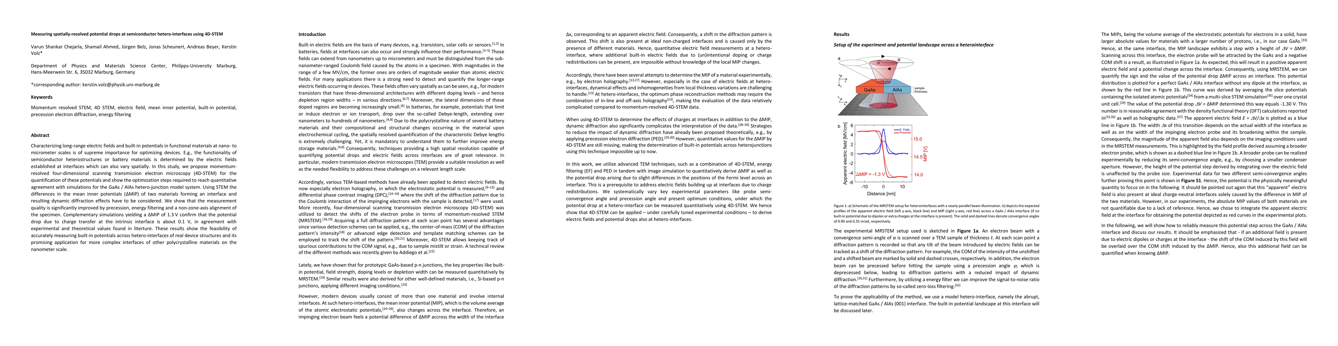
Characterizing long-range electric fields and built-in potentials in functional materials at nano- to micrometer scales is of supreme importance for optimizing devices. E.g., the functionality of semiconductor heterostructures or battery materials is determined by the electric fields established at interfaces which can also vary spatially. In this study, we propose momentum-resolved four-dimensional scanning transmission electron microscopy (4D-STEM) for the quantification of these potentials and show the optimization steps required to reach quantitative agreement with simulations for the GaAs / AlAs hetero-junction model system. Using STEM the differences in the mean inner potentials (DELTA MIP) of two materials forming an interface and resulting dynamic diffraction effects have to be considered. We show that the measurement quality is significantly improved by precession, energy filtering and a non-zone-axis alignment of the specimen. Complementary simulations yielding a DELTA MIP of 1.3 V confirm that the potential drop due to charge transfer at the intrinsic interface is about 0.1 V, in agreement with experimental and theoretical values found in literture. These results show the feasibility of accurately measuring built-in potentials across hetero-interfaces of real device structures and its promising application for more complex interfaces of other polycrystalline materials on the nanometer scale.
Seven facets of this paper, analysed and brought into focus by AI.
Why this research is important and its potential impact
Brief description of the research methodology used
Why this research is important and its potential impact
Main technical or theoretical contribution
What makes this work novel or different from existing research
Current paper (gray), citations (green), references (blue)
Display is limited for performance on very large graphs.
Discussion 0