Academic Profile
Statistics
Similar Authors
Papers on arXiv
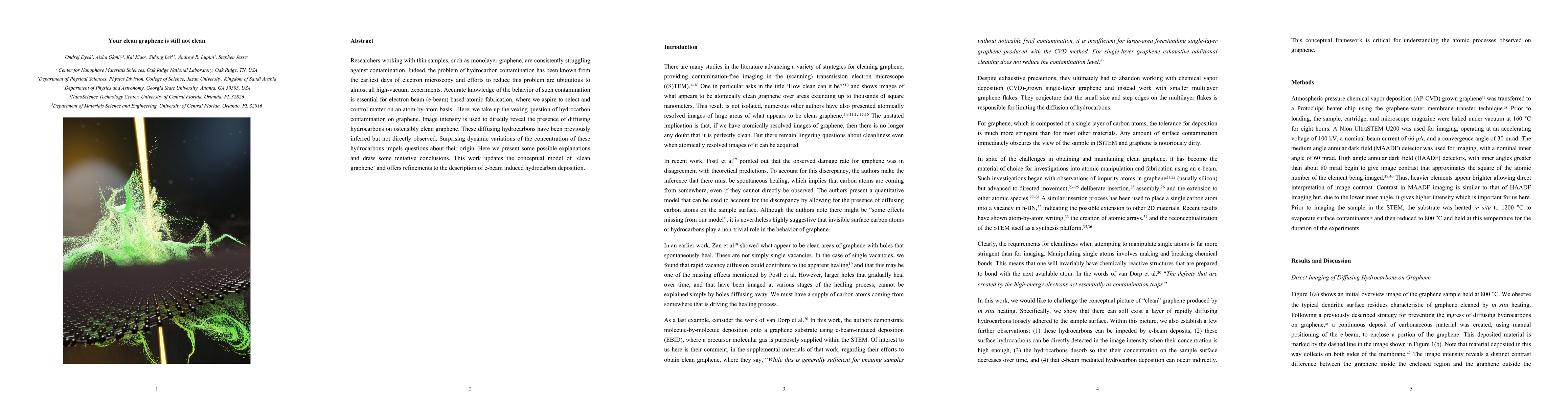
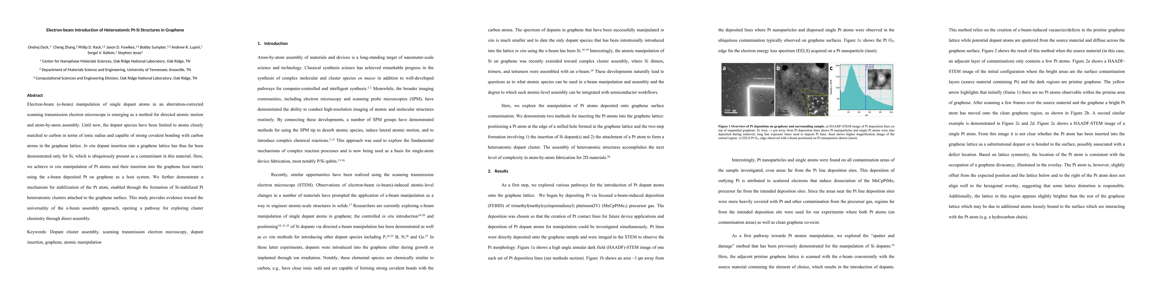
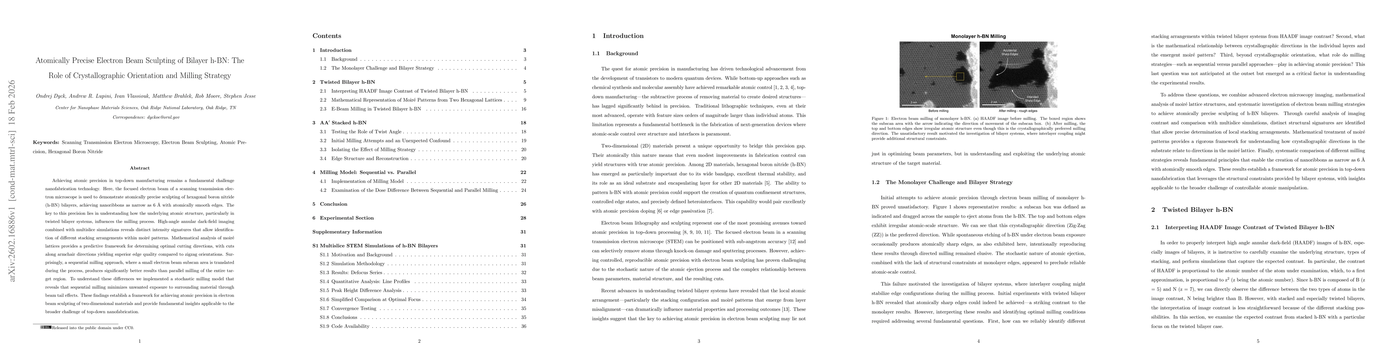
Efforts aimed at scaling fabrication processes to the level of single atoms, dubbed atom-by-atom fabrication or atomic fabrication, invariably encounter the obstacle of atomic scale cleanliness. Whe...
Structural disorder has been shown to enhance and modulate magnetic, electrical, dipolar, electrochemical, and mechanical properties of materials. However, the possibility of obtaining novel optical...
Focused electron beam induced deposition (FEBID) is a direct write technique for depositing materials on a support substrate akin to 3D printing with an electron beam (e-beam). Opportunities exist f...
Atomic-scale fabrication is an outstanding challenge and overarching goal for the nanoscience community. The practical implementation of moving and fixing atoms to a structure is non-trivial conside...
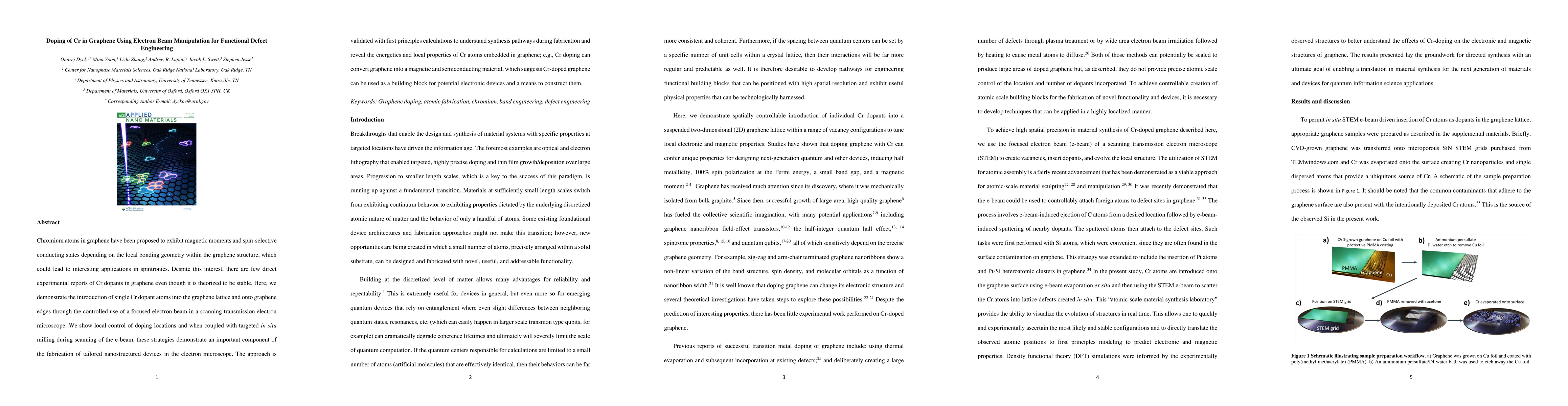
Chromium atoms in graphene have been proposed to exhibit magnetic moments and spin-selective conducting states depending on the local bonding geometry within the graphene structure, which could lead...

Graphene is of great scientific interest due to a variety of unique properties such as ballistic transport, spin selectivity, the quantum hall effect, and other quantum properties. Nanopatterning an...
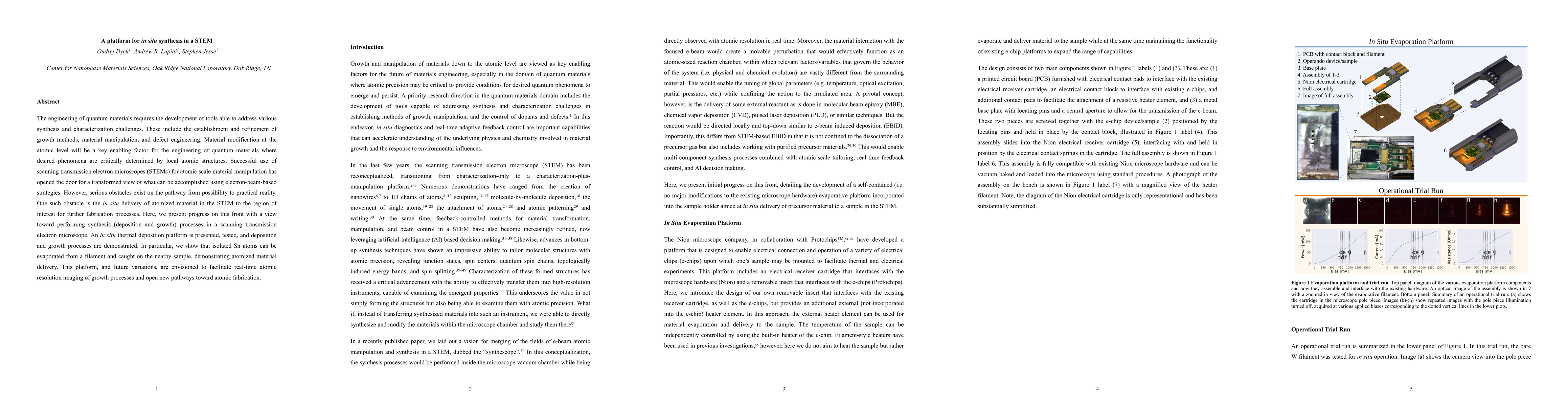
The engineering of quantum materials requires the development of tools able to address various synthesis and characterization challenges. These include the establishment and refinement of growth met...
The performance of electron energy-loss spectrometers can often be limited by their electron-optical aberrations. Due to recent developments in high energy-resolution and momentum-resolved electron ...
Electronic states within superconducting vortices hold crucial information about paring mechanisms and topology. While scanning tunneling microscopy/spectroscopy(STM/S) can image the vortices, it is...
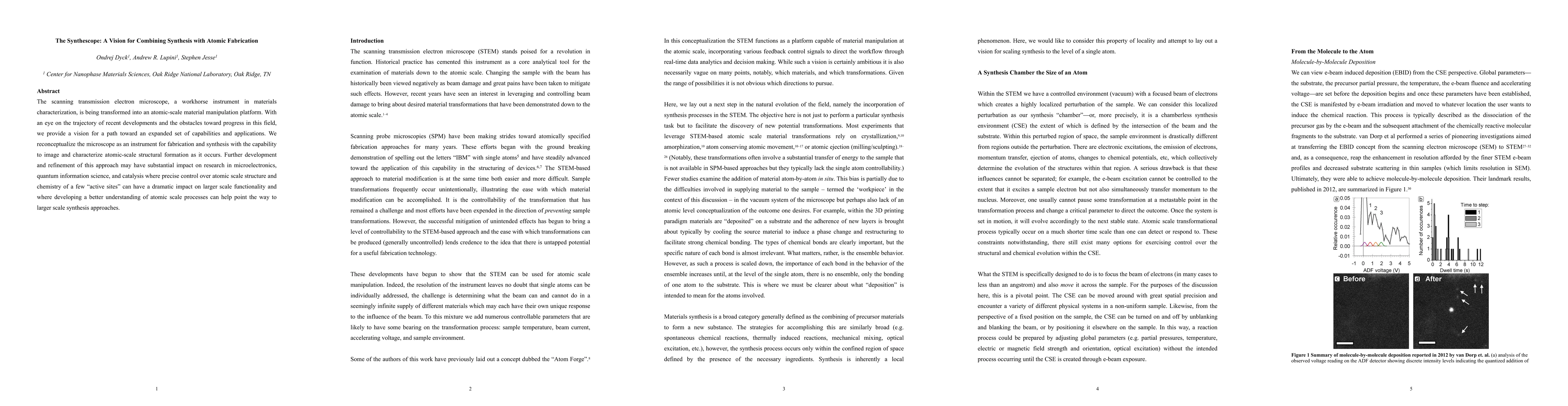
The scanning transmission electron microscope, a workhorse instrument in materials characterization, is being transformed into an atomic-scale material manipulation platform. With an eye on the traj...
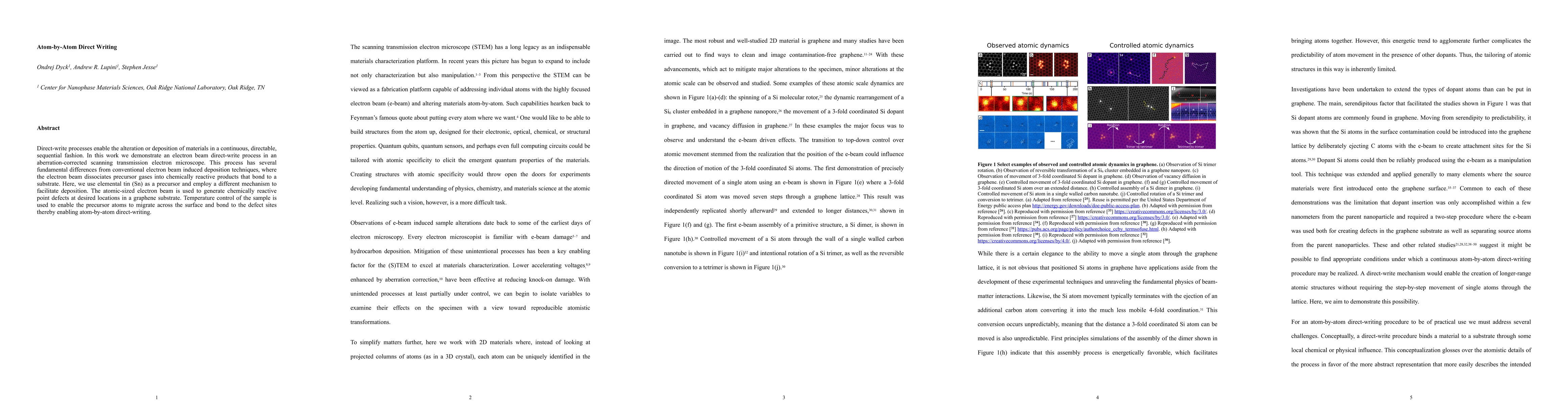
Direct-write processes enable the alteration or deposition of materials in a continuous, directable, sequential fashion. In this work we demonstrate an electron beam direct-write process in an aberr...
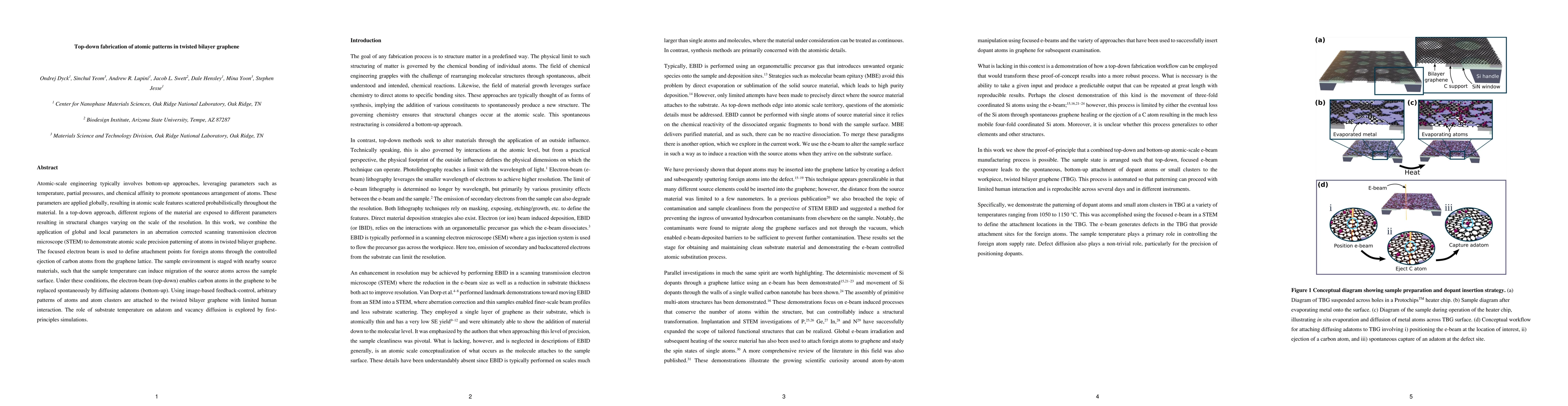
Atomic-scale engineering typically involves bottom-up approaches, leveraging parameters such as temperature, partial pressures, and chemical affinity to promote spontaneous arrangement of atoms. The...
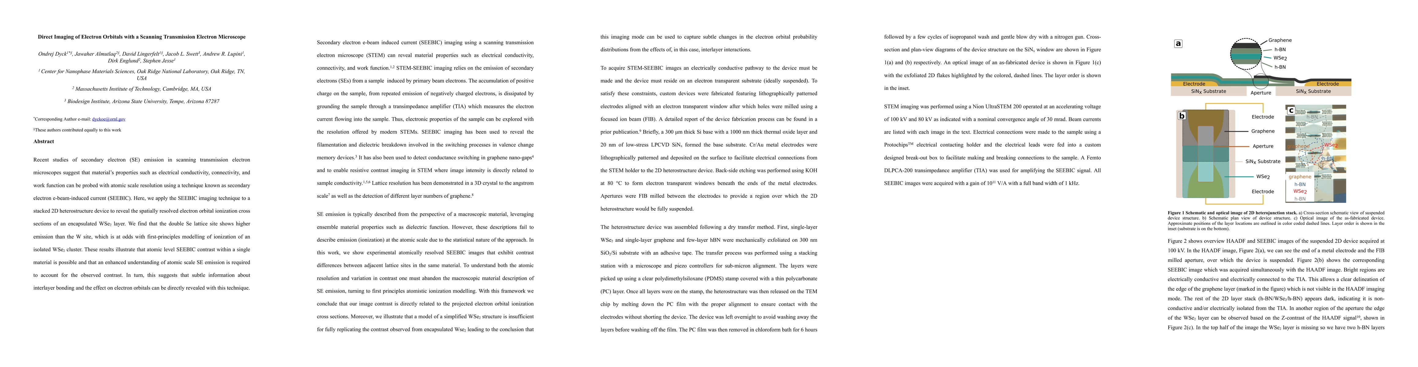
Recent studies of secondary electron (SE) emission in scanning transmission electron microscopes suggest that material's properties such as electrical conductivity, connectivity, and work function c...
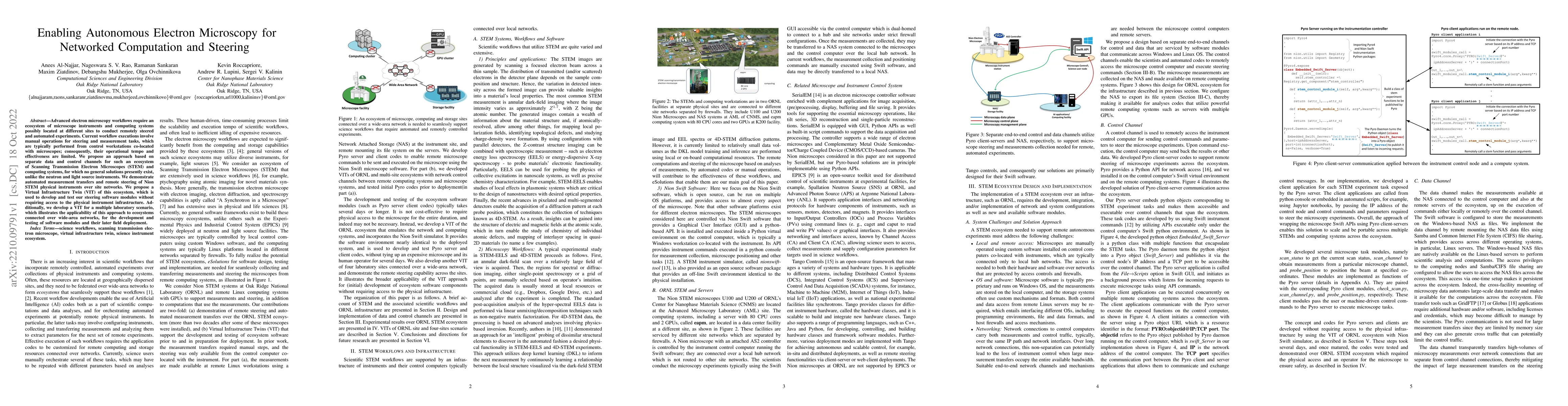
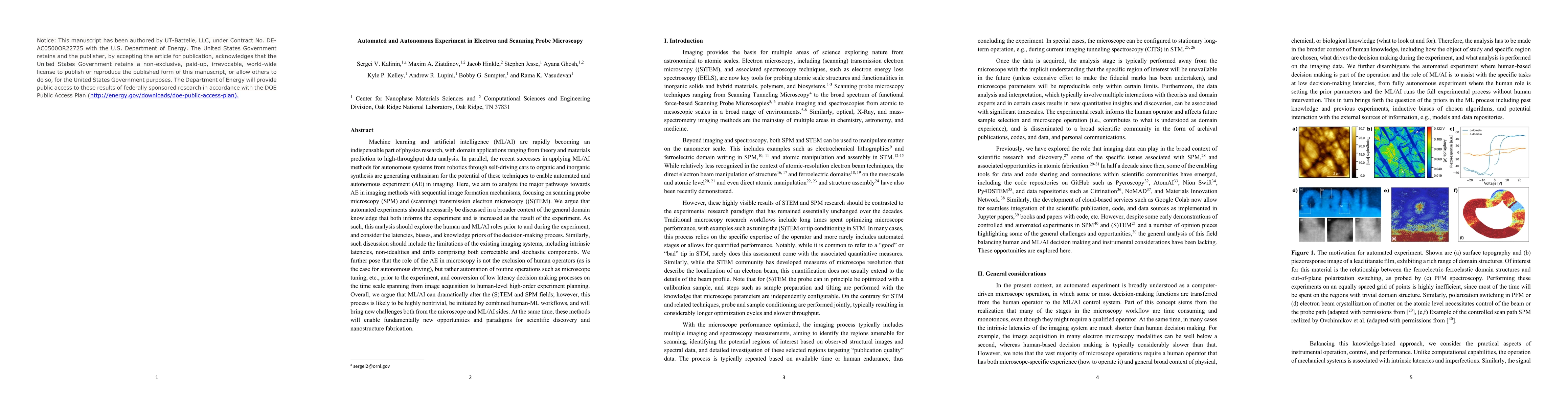
Advanced electron microscopy workflows require an ecosystem of microscope instruments and computing systems possibly located at different sites to conduct remotely steered and automated experiments....
The advent of modern, high-speed electron detectors has made the collection of multidimensional hyperspectral transmission electron microscopy datasets, such as 4D-STEM, a routine. However, many mic...
Electron-beam (e-beam) manipulation of single dopant atoms in an aberration-corrected scanning transmission electron microscope is emerging as a method for directed atomic motion and atom-by-atom as...
Graphene has been proposed for use in various nanodevice designs, many of which harness emergent quantum properties for device functionality. However, visualization, measurement, and manipulation be...
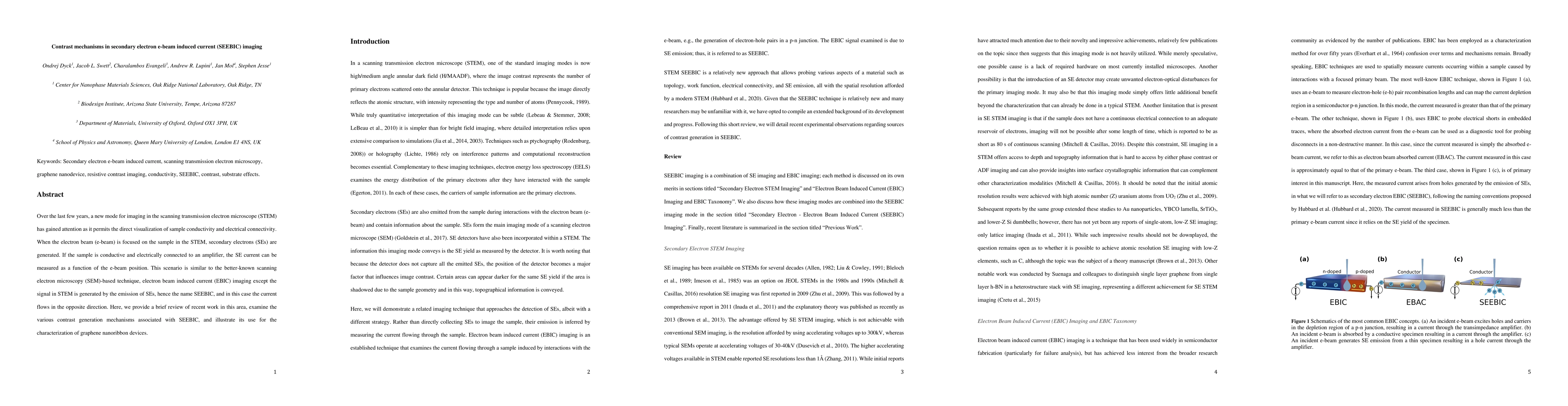
Over the last few years, a new mode for imaging in the scanning transmission electron microscope (STEM) has gained attention as it permits the direct visualization of sample conductivity and electri...
Over the last two decades, Electron Energy Loss Spectroscopy (EELS) imaging with a scanning transmission electron microscope (STEM) has emerged as a technique of choice for visualizing complex chemi...
Elucidating the symmetry of intertwined orders in exotic superconductors is at the quantum frontier. Recent surface sensitive studies of the topological kagome superconductor CsV$_3$Sb$_5$ discovere...
Quantum materials (QMs) with strong correlation and non-trivial topology are indispensable to next-generation information and computing technologies. Exploitation of topological band structure is an...
Hexagonal perovskites are an attractive group of materials due to their various polymorph phases and rich structure-property relationships. BaRuO3 (BRO) is a prototypical hexagonal perovskite, in wh...
Twin domains are often found as structural defects in symmetry mismatched epitaxial thin films. The delafossite ABO2, which has a rhombohedral structure, is a good example that often forms twin doma...
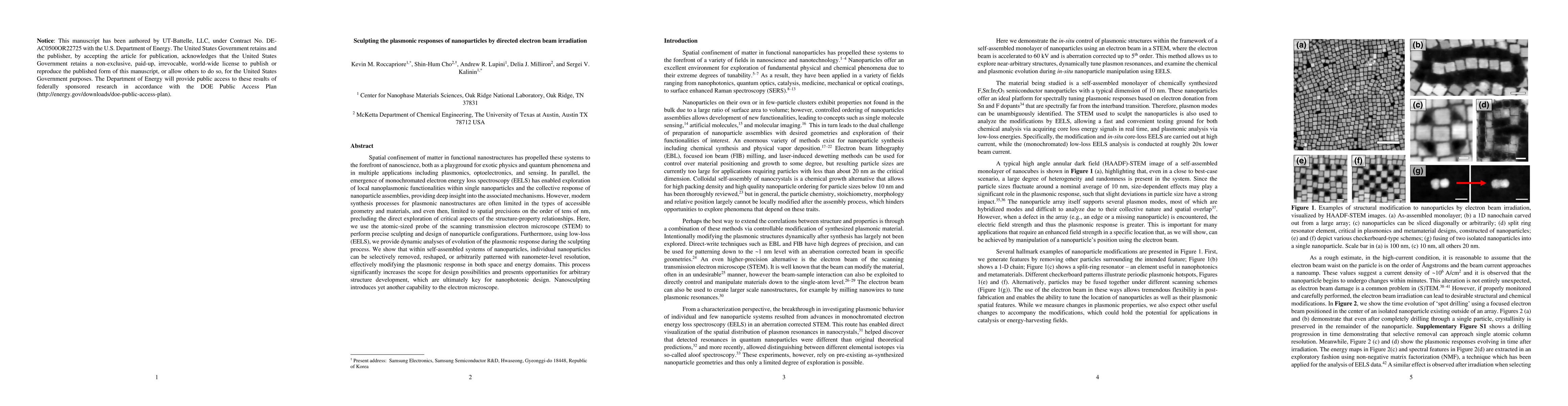
Spatial confinement of matter in functional nanostructures has propelled these systems to the forefront of nanoscience, both as a playground for exotic physics and quantum phenomena and in multiple ...
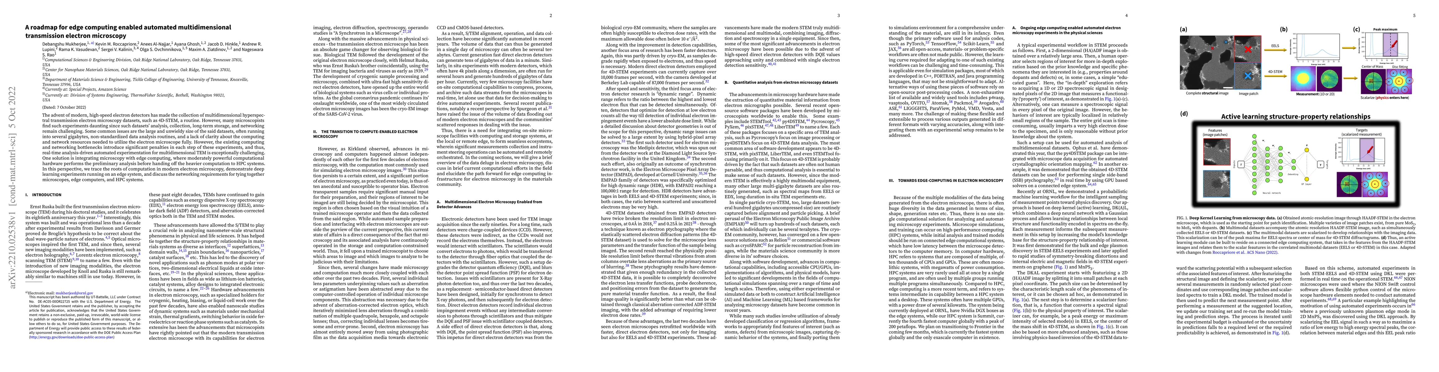
Machine learning and artificial intelligence (ML/AI) are rapidly becoming an indispensable part of physics research, with domain applications ranging from theory and materials prediction to high-thr...
The 4D scanning transmission electron microscopy (STEM) method has enabled mapping of the structure and functionality of solids on the atomic scale, yielding information-rich data sets containing in...
Advances in hyperspectral imaging modes including electron energy loss spectroscopy (EELS) in scanning transmission electron microscopy (STEM) bring forth the challenges of exploratory and subsequen...
Interface structures in complex oxides remain one of the active areas of condensed matter physics research, largely enabled by recent advances in scanning transmission electron microscopy (STEM). Ye...
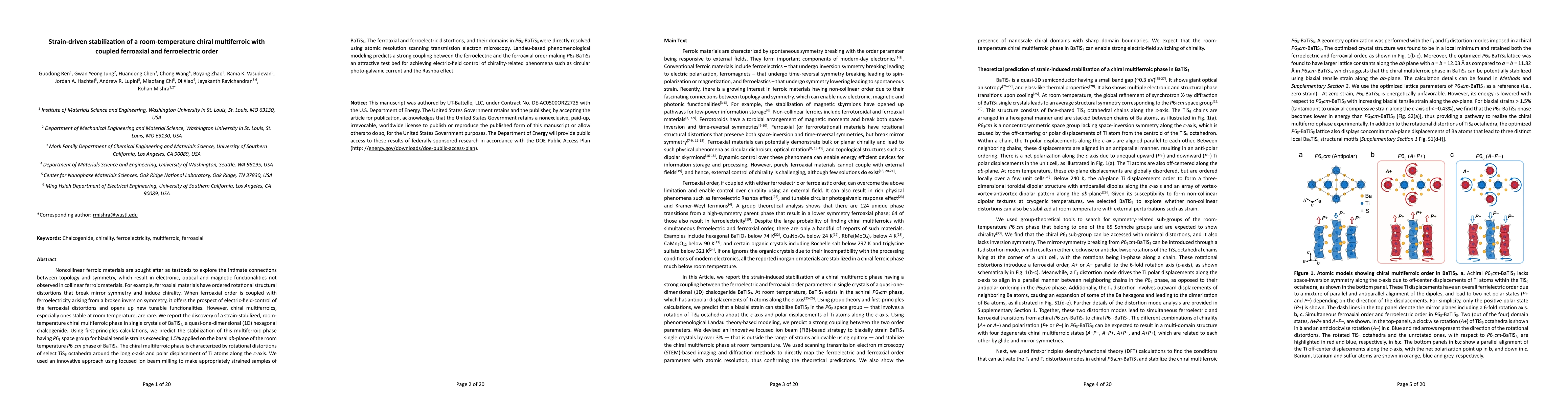
Noncollinear ferroic materials are sought after as testbeds to explore the intimate connections between topology and symmetry, which result in electronic, optical and magnetic functionalities not obse...
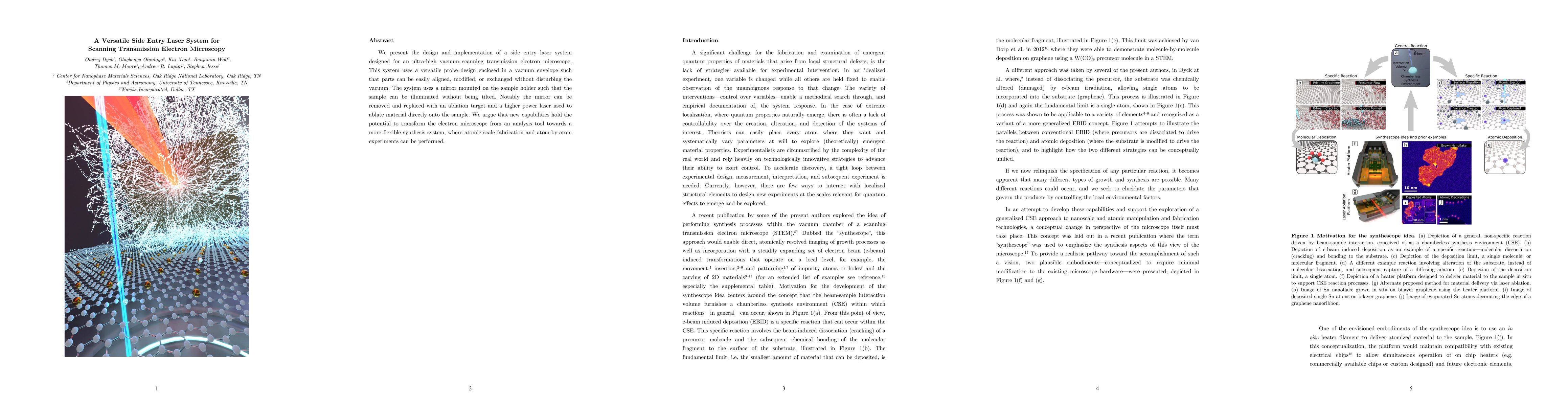
We present the design and implementation of a side entry laser system designed for an ultra-high vacuum scanning transmission electron microscope. This system uses a versatile probe design enclosed in...
The discovery of ferroelectricity in hafnia-based materials have boosted the potential of incorporating ferroelectrics in advanced electronics, thanks to their compatibility with silicon technology. H...
Recently, numerous techniques have been reported for generating optically active defects in exfoliated hexagonal boron nitride (hBN), which hold transformative potential for quantum photonic devices. ...
Optically anisotropic materials are sought after for tailoring the polarization of light. Recently, colossal optical anisotropy was reported in a quasi-one-dimensional chalcogenide, Sr1.125TiS3. Compa...
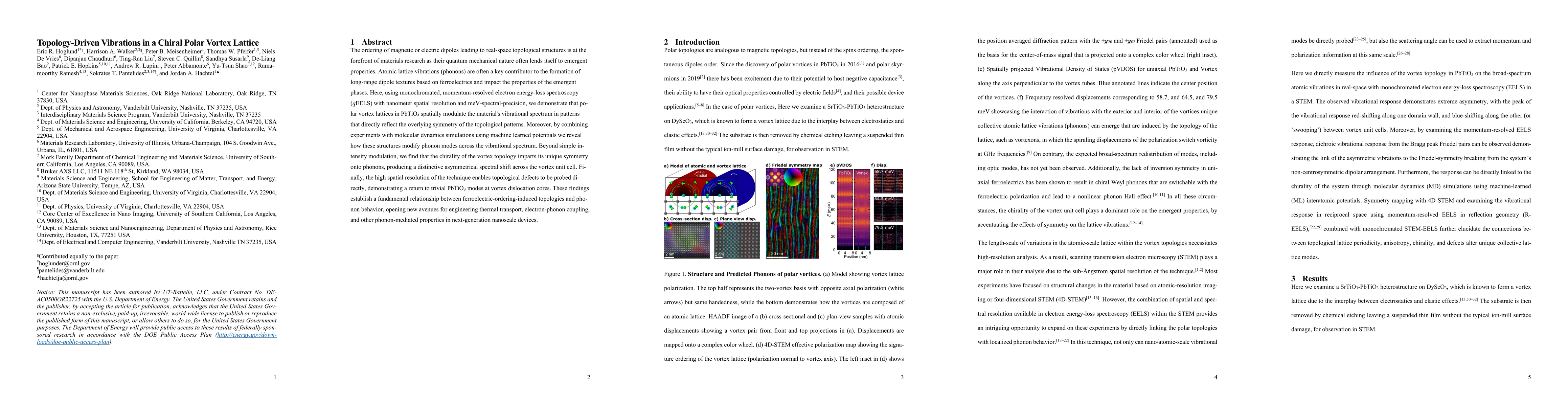
The ordering of magnetic or electric dipoles leading to real-space topological structures is at the forefront of materials research as their quantum mechanical nature often lends itself to emergent pr...
Achieving atomic precision in top-down manufacturing remains a fundamental challenge nanofabrication technology. Here, the focused electron beam of a scanning transmission electron microscope is used ...
Four-dimensional scanning transmission electron microscopy (4D-STEM) generates multi-gigabyte datasets, creating a growing mismatch between acquisition rates and practical storage, transfer, and inter...