This paper reviews recent advancements in secondary electron e-beam induced current (SEEBIC) imaging in scanning transmission electron microscopes (STEM), contrasting its mechanisms with electron beam induced current (EBIC) imaging. It highlights SEEBIC's utility in visualizing sample conductivity and its application in characterizing graphene nanoribbon devices.
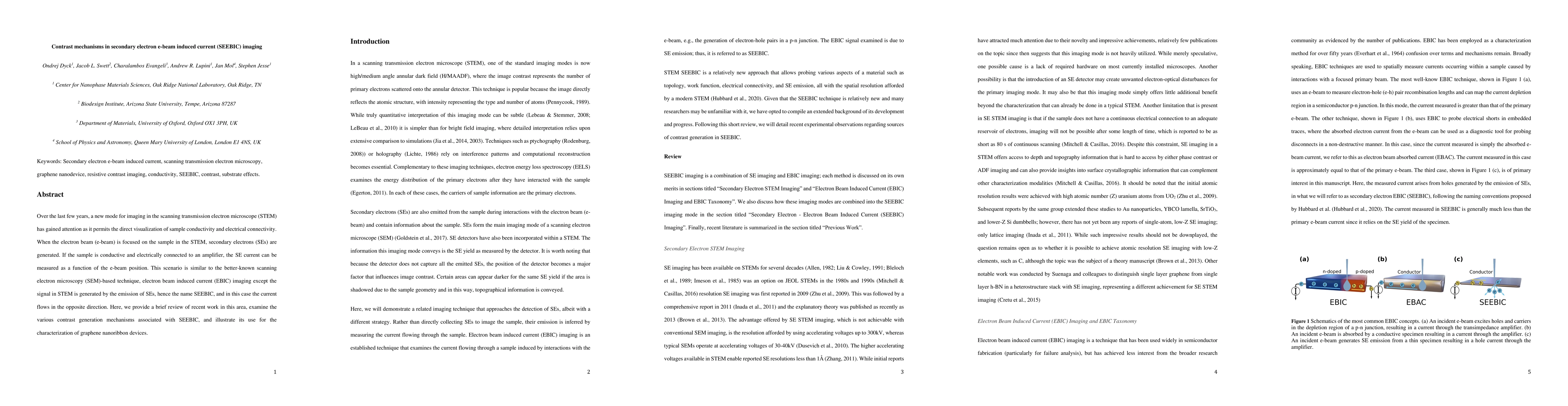
Over the last few years, a new mode for imaging in the scanning transmission electron microscope (STEM) has gained attention as it permits the direct visualization of sample conductivity and electrical connectivity. When the electron beam (e-beam) is focused on the sample in the STEM, secondary electrons (SEs) are generated. If the sample is conductive and electrically connected to an amplifier, the SE current can be measured as a function of the e-beam position. This scenario is similar to the better-known scanning electron microscopy (SEM)-based technique, electron beam induced current (EBIC) imaging except the signal in STEM is generated by the emission of SEs, hence the name SEEBIC, and in this case the current flows in the opposite direction. Here, we provide a brief review of recent work in this area, examine the various contrast generation mechanisms associated with SEEBIC, and illustrate its use for the characterization of graphene nanoribbon devices.
Get AI-generated insights about this paper's methodology, results, and significance.
Current paper (gray), citations (green), references (blue)
Ondrej Dyck, Andrew R. Lupini, Stephen Jesse et al.
Title | Authors | Year | Actions |
---|---|---|---|
The role of primary and secondary electrons in scanning transmission electron microscopy of hybrid perovskites: the CsPbBr$_{3}$ case
|
P. E. Trevisanutto, S. Taioli, M. Dapor, C. S. Allen, G. Teobaldi
|
2024
|
View Paper |
Direct Imaging of Electron Orbitals with a Scanning Transmission Electron Microscope
|
Ondrej Dyck, Jawaher Almutlaq, J. Swett, A. Lupini, D. Englund, S. Jesse
|
2022
|
View Paper |
Title | Authors | Year | Actions |
---|---|---|---|
Mapping Conductance and Switching Behavior of Graphene Devices In Situ
|
Ondrej Dyck, J. Swett, C. Evangeli, A. Lupini, J. Mol, S. Jesse
|
2021
|
View Paper |
Imaging Secondary Electron Emission from a Single Atomic Layer.
|
O. Dyck, J. Swett, A. Lupini, J. Mol, S. Jesse
|
2021
|
View Paper |
Single-electron spin resonance in a nanoelectronic device using a global field
|
E. Vahapoglu, J. Slack-Smith, R. Leon, W. H. Lim, F. Hudson, Tom Day, T. Tanttu, C. Yang, A. Laucht, A. Dzurak, J. Pla
|
2020
|
View Paper |
STEM electron beam-induced current measurements of organic-inorganic perovskite solar cells.
|
M. Duchamp, H. Hu, Y. Lam, R. Dunin‐Borkowski, C. Boothroyd
|
2020
|
View Paper |
In Situ 2D MoS2 Field Effect Transistors with an Electron Beam Gate.
|
Paul Masih Das, M. Drndić
|
2020
|
View Paper |
STEM EBIC for High-Resolution Electronic Characterization
|
W. Hubbard, Z. Lingley, J. Theiss, M. Brodie, B. Foran
|
2020
|
View Paper |
Electron beam-induced current imaging with two-angstrom resolution.
|
M. Mecklenburg, W. Hubbard, J. Lodico, B. Regan
|
2019
|
View Paper |
Scanning transmission electron microscope mapping of electronic transport in polycrystalline BaTiO3 ceramic capacitors
|
William A Hubbard, Z. Lingley, Jesse Theiss, Scott D. Sitzman, Talin Ayvazian, M. Brodie, Brendan Foran
|
2019
|
View Paper |
Adjusting the STEM Sample Holder Potential for Improved EBIC Contrast
|
M. Mecklenburg, W. Hubbard, H. Chan, B. Regan
|
2019
|
View Paper |
Fabrication and practical applications of molybdenum disulfide nanopores
|
M. Graf, Martina Lihter, M. Thakur, Vasileia Georgiou, Vasileia Georgiou, Juraj Topolancik, Juraj Topolancik, B. Ilic, Ke Liu, Jiandong Feng, Y. Astier, A. Radenović
|
2019
|
View Paper |
Measuring the areal density of nanomaterials by electron energy-loss spectroscopy.
|
M. Tian, O. Dyck, J. Ge, G. Duscher
|
2019
|
View Paper |
STEM Imaging with Beam-Induced Hole and Secondary Electron Currents
|
W. Hubbard, M. Mecklenburg, H. Chan, B. Regan
|
2018
|
View Paper |
In Situ Room Temperature Electron-Beam Driven Graphene Growth from Hydrocarbon Contamination in a Transmission Electron Microscope
|
M. Rummeli, Yuanan Pan, Liang Zhao, Jing Gao, Huy Q. Ta, I. G. Martinez, R. Mendes, T. Gemming, L. Fu, A. Bachmatiuk, Zhongfan Liu
|
2018
|
View Paper |
Compressed Sensing of Scanning Transmission Electron Microscopy (STEM) With Nonrectangular Scans
|
Xin Li, O. Dyck, Sergei V. Kalinin, S. Jesse
|
2018
|
View Paper |
Nonlinear optics on silicon-rich nitride—a high nonlinear figure of merit CMOS platform [Invited]
|
D. Tan, K. Ooi, D. Ng
|
2018
|
View Paper |
Trainable Weka Segmentation: a machine learning tool for microscopy pixel classification
|
Ignacio Arganda-Carreras, V. Kaynig, C. Rueden, K. Eliceiri, J. Schindelin, Albert Cardona, H. Seung
|
2017
|
View Paper |
Precision controlled atomic resolution scanning transmission electron microscopy using spiral scan pathways
|
X. Sang, A. Lupini, J. Ding, Sergei V. Kalinin, S. Jesse, R. Unocic
|
2017
|
View Paper |
Secondary Electron Imaging in an Aberration-Corrected STEM
|
D. Mitchell, G. Casillas
|
2016
|
View Paper |
Dynamic scan control in STEM: spiral scans
|
X. Sang, A. Lupini, R. Unocic, M. Chi, A. Borisevich, Sergei V. Kalinin, E. Endeve, R. Archibald, S. Jesse
|
2016
|
View Paper |
Imaging interfacial electrical transport in graphene-MoS2 heterostructures with electron-beam-induced-currents.
|
E. White, A. Kerelsky, W. Hubbard, R. Dhall, S. Cronin, M. Mecklenburg, B. Regan
|
2015
|
View Paper |
Electron beam induced current on carbon nanotubes measured through substrate electrodes
|
Ji-Yong Park, Y. Ahn
|
2015
|
View Paper |
Secondary electron imaging of monolayer materials inside a transmission electron microscope
|
O. Cretu, Yung‐Chang Lin, K. Suenaga
|
2015
|
View Paper |
Poole-Frenkel-effect as dominating current mechanism in thin oxide films—An illusion?!
|
H. Schroeder
|
2015
|
View Paper |
Conductance enlargement in picoscale electroburnt graphene nanojunctions
|
H. Sadeghi, J. Mol, C. Lau, Andrew Briggs, J. Warner, C. Lambert
|
2015
|
View Paper |
In Situ TEM Imaging of Defect Dynamics under Electrical Bias in Resistive Switching Rutile-TiO2
|
R. Kamaladasa, Abhishek A. Sharma, Yu-Ting Lai, Wenhao Chen, P. Salvador, J. Bain, M. Skowronski, Y. Picard
|
2014
|
View Paper |
Determination of the 3D shape of a nanoscale crystal with atomic resolution from a single image.
|
C. Jia, C. Jia, C. Jia, S. Mi, J. Barthel, J. Barthel, Dawei Wang, R. Dunin‐Borkowski, R. Dunin‐Borkowski, K. Urban, K. Urban, A. Thust, A. Thust
|
2014
|
View Paper |
Nanoscale control of graphene electrodes.
|
C. Lau, J. Mol, Jh H. Warner, G. Briggs
|
2014
|
View Paper |
Toward sensitive graphene nanoribbon-nanopore devices by preventing electron beam-induced damage.
|
M. Puster, J. A. Rodríguez-Manzo, A. Balan, M. Drndić
|
2013
|
View Paper |
Spatially resolved mapping of electrical conductivity across individual domain (grain) boundaries in graphene.
|
K. Clark, X-G Zhang, I. Vlassiouk, Guowei He, R. Feenstra, An‐Ping Li
|
2013
|
View Paper |
Secondary electron imaging at atomic resolution using a focused coherent electron probe
|
H. Brown, A. J. D’Alfonso, L. Allen
|
2013
|
View Paper |
Batch-fabricated high-performance graphene Hall elements
|
Huilong Xu, Zhiyong Zhang, R. Shi, Honggang Liu, Zhenxing Wang, Sheng Wang, Lianmao Peng
|
2013
|
View Paper |
Electronics and optoelectronics of two-dimensional transition metal dichalcogenides.
|
Qing Hua Wang, K. Kalantar-zadeh, A. Kis, J. Coleman, M. Strano
|
2012
|
View Paper |
Fiji: an open-source platform for biological-image analysis
|
J. Schindelin, Ignacio Arganda-Carreras, E. Frise, V. Kaynig, M. Longair, T. Pietzsch, S. Preibisch, C. Rueden, S. Saalfeld, Benjamin Schmid, J. Tinevez, D. J. White, V. Hartenstein, K. Eliceiri, P. Tomančák, Albert Cardona
|
2012
|
View Paper |
Room-temperature gating of molecular junctions using few-layer graphene nanogap electrodes.
|
F. Prins, A. Barreiro, Justus W. Ruitenberg, J. S. Seldenthuis, N. Aliaga-Alcalde, L. Vandersypen, H. V. D. van der Zant
|
2011
|
View Paper |
A 200-kV STEM/SEM Produces 1 Å SEM Resolution
|
Xiao Feng Zhang
|
2011
|
View Paper |
Single-layer MoS2 transistors.
|
B. Radisavljevic, A. Radenović, J. Brivio, V. Giacometti, A. Kis
|
2011
|
View Paper |
Response to “Comment on ‘Ultrahigh secondary electron emission of carbon nanotubes’ ” [Appl. Phys. Lett. 98, 066101 (2011)]
|
Jun Luo, J. Warner, G. Briggs
|
2011
|
View Paper |
Comment on “Ultrahigh secondary electron emission of carbon nanotubes” [Appl. Phys. Lett. 96, 213113 (2010)]
|
Md. Kawsar Alam, R. Pease, A. Nojeh
|
2011
|
View Paper |
Standardless atom counting in scanning transmission electron microscopy.
|
J. Lebeau, S. Findlay, L. Allen, S. Stemmer
|
2010
|
View Paper |
Atomic imaging using secondary electrons in a scanning transmission electron microscope: experimental observations and possible mechanisms.
|
H. Inada, D. Su, R. Egerton, M. Konno, Lijun Wu, J. Ciston, J. Wall, Yimei Zhu
|
2010
|
View Paper |
Ultrahigh secondary electron emission of carbon nanotubes
|
Jun Luo, J. Warner, Chaoqun Feng, Yagang Yao, Zhong Jin, Huiliang Wang, Caofeng Pan, Sheng Wang, Leijing Yang, Yan Li, Jin Zhang, A. Watt, Lianmao Peng, Jing Zhu, G. Briggs
|
2010
|
View Paper |
Electron beam induced current measurements on single-walled carbon nanotube devices
|
Jae-Soung Park, Y. H. Ahn, Ji-Yong Park, Soonil Lee, Kwan-Ho Park
|
2010
|
View Paper |
Choosing the Right Accelerating Voltage for SEM (An Introduction for Beginners)
|
V. Dusevich, Purk Jh, J. Eick
|
2010
|
View Paper |
Imaging single atoms using secondary electrons with an aberration-corrected electron microscope.
|
Yan Zhu, H. Inada, K. Nakamura, J. Wall
|
2009
|
View Paper |
Logic failure analysis 65/45nm device using RCI & nano scale probe
|
S.J. Cho, T.E. Kim, J.K. Hong, J.T. Hong, H. Kim, Y.W. Han, S. Kwon, Y. Oh
|
2009
|
View Paper |
Experimental quantification of annular dark-field images in scanning transmission electron microscopy.
|
J. Lebeau, S. Stemmer
|
2008
|
View Paper |
ELECTRON EMISSION FROM CARBON NANOTUBES
|
P. Yaghoobi, A. Nojeh
|
2007
|
View Paper |
Sub-10 nm device fabrication in a transmission electron microscope.
|
M. D. Fischbein, M. Drndić
|
2007
|
View Paper |
A new examination of secondary electron yield data
|
Yinghong Lin, D. Joy
|
2005
|
View Paper |
Atomic-Resolution Imaging of Oxygen in Perovskite Ceramics
|
Chun-Lin Jia, M. Lentzen, K. Urban
|
2003
|
View Paper |
Correlation of charge transport to local atomic strain in Si-rich silicon nitride thin films
|
S. Habermehl, C. Carmignani
|
2002
|
View Paper |
LPCVD and PECVD silicon nitride for microelectronics technology
|
B. C. Joshi, G. Eranna, D. P. Runthala, B. Dixit, O. P. Wadhawan, P. Vyas
|
2000
|
View Paper |
Stress relaxation in Si-rich silicon nitride thin films
|
S. Habermehl
|
1998
|
View Paper |
Structural properties of N-rich a-Si - N:H films with a low electron-trapping rate
|
G. Dupont, H. Caquineau, B. Despax, R. Berjoan, A. Dollet
|
1997
|
View Paper |
Scanning transmission electron beam induced conductivity investigation of a Si/Si1−xGex/Si heterostructure
|
P. Brown, C. Humphreys
|
1996
|
View Paper |
Electron Energy-Loss Spectroscopy in the Electron Microscope
|
R. Egerton
|
1995
|
View Paper |
Scanning Electron Microscopy and X-Ray Microanalysis
|
Robert Edward Lee
|
1992
|
View Paper |
Imaging with high-angle scattered electrons and secondary electrons in the STEM
|
J. Liu, J. Cowley
|
1991
|
View Paper |
Growth and electronic properties of thin Si3N4 films grown on Si in a nitrogen glow discharge
|
E. Paloura, J. Lagowski, H. Gatos
|
1991
|
View Paper |
High resolution secondary electron imaging and spectroscopy
|
A. Bleloch, A. Howie, R. Milne
|
1989
|
View Paper |
Resistive contrast imaging applied to multilevel interconnection failure analysis
|
E. I. Cole
|
1989
|
View Paper |
Z-contrast stem for materials science
|
S. Pennycook
|
1989
|
View Paper |
Resistive contrast imaging: A new SEM mode for failure analysis
|
C. A. Smith, C. R. Bagnell, E. I. Cole, F. DiBianca, D. G. Johnson, W. V. Oxford, R. H. Propst
|
1986
|
View Paper |
Gap states in silicon nitride
|
J. Robertson, M. J. Powell
|
1984
|
View Paper |
Secondary electron emission in the scanning electron microscope
|
H. Seiler
|
1983
|
View Paper |
Variation in the stoichiometry of thin silicon nitride insulating films on silicon and its correlation with memory traps
|
R. Bailey, V. Kapoor
|
1982
|
View Paper |
Observation of dislocations and microplasma sites in semiconductors by direct correlations of STEBIC, STEM and ELS
|
D. Fathy, T. Sparrow, U. Valdré
|
1980
|
View Paper |
Application of scanning transmission electron microscopy to semiconductor devices
|
T. Sparrow, U. Valdrèg
|
1977
|
View Paper |
Secondary electron emission from thin carbon films
|
D. Voreades
|
1976
|
View Paper |
Current Transport and Maximum Dielectric Strength of Silicon Nitride Films
|
S. Sze
|
1967
|
View Paper |
Evaluation of Passivated Integrated Circuits Using the Scanning Electron Microscope
|
T. Everhart, O. Wells, R. Matta
|
1964
|
View Paper |
Electron beam damage in oxides: a review
|
N. Jiang
|
2016
|
View Paper |
Electro-optical Properties of Non-stoichiometric Silicon Nitride Films for Photovoltaic Applications
|
O. Blázquez, J. López-Vidrier, S. Hernández, J. Montserrat, B. Garrido
|
2014
|
View Paper |
Ptychography and Related Diffractive Imaging Methods
|
J. Rodenburg
|
2008
|
View Paper |
Failure Analysis of Integrated Circuits
|
L. C. Wagner
|
1999
|
View Paper |
Problems associated with imaging resistive barriers in BaTiO3 PTC ceramics using the SEM conductive mode
|
J. D. Russell, C. Leach
|
1995
|
View Paper |
Electron holography approaching atomic resolution
|
H. Lichte
|
1986
|
View Paper |
Secondary electron detection in the scanning transmission electron microscope
|
D. Imeson, R. Milne, S. Berger, D. Mcmullan
|
1985
|
View Paper |
Secondary electron imaging as an aid to STEM microanalysis
|
R. Allen
|
1982
|
View Paper |
Correlating Atomic Structure and Transport in Suspended Graphene Nanoribbons
|
2014
|
||
https://doi.org/10.1017/S1431927622000824 Published online by Cambridge University
|
2000
|
||
Direct electron beam patterning of sub-5 nm monolayer graphene interconnects
|
2013
|
Showing first page preview. Click "Open Full PDF" to view the complete paper.
Your comment contains inappropriate language and has been rejected.
Are you sure you want to remove this tag? This action cannot be undone.
Someone just favorited a paper!
Comments (0)