Academic Profile
Statistics
Similar Authors
Papers on arXiv
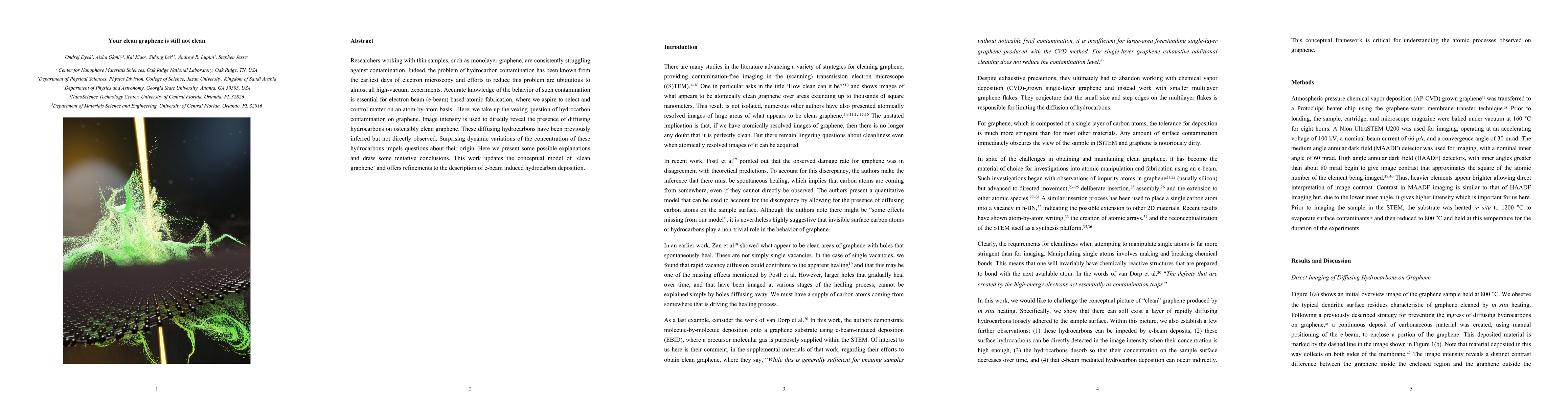
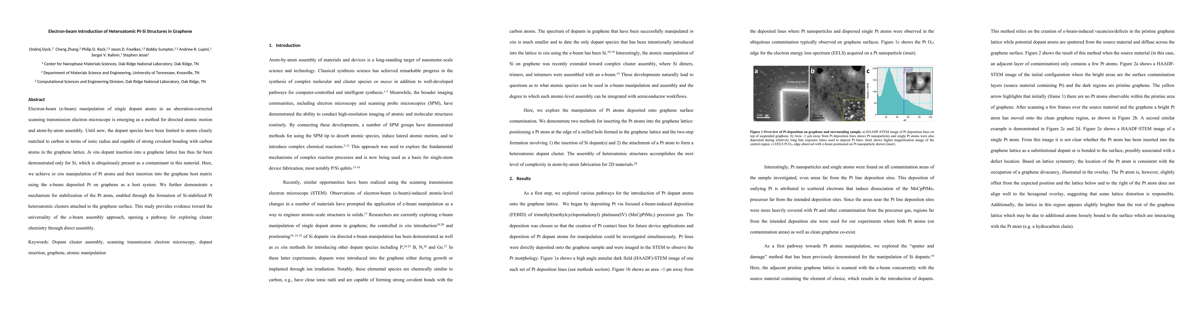
Efforts aimed at scaling fabrication processes to the level of single atoms, dubbed atom-by-atom fabrication or atomic fabrication, invariably encounter the obstacle of atomic scale cleanliness. Whe...
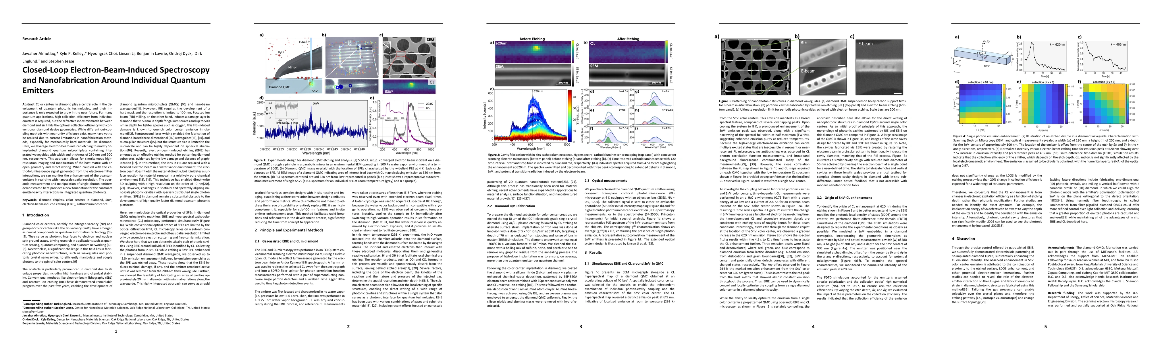
Color centers in diamond play a central role in the development of quantum photonic technologies, and their importance is only expected to grow in the near future. For many quantum applications, hig...
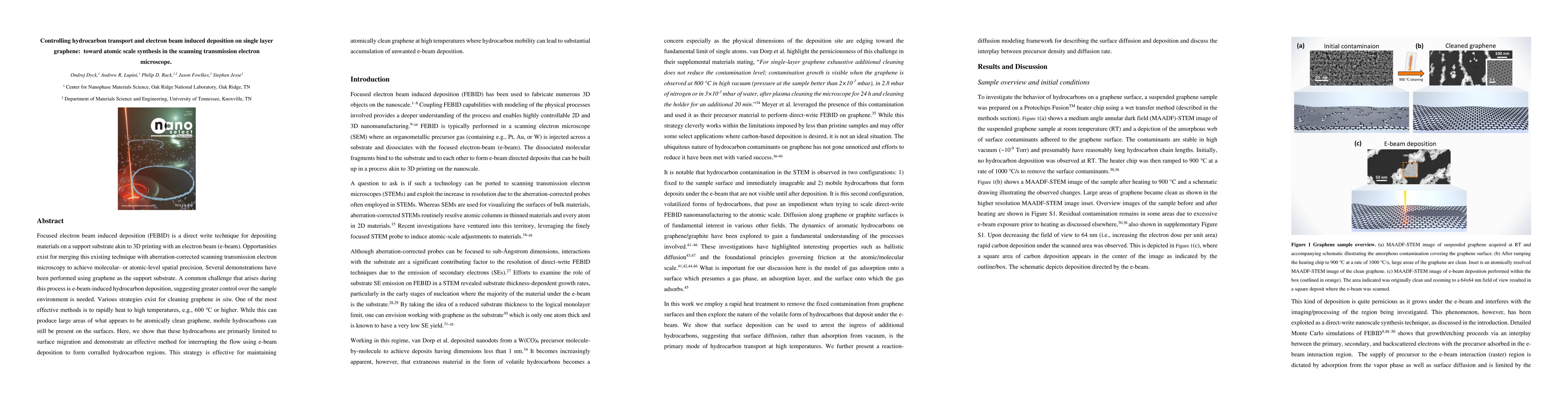
Focused electron beam induced deposition (FEBID) is a direct write technique for depositing materials on a support substrate akin to 3D printing with an electron beam (e-beam). Opportunities exist f...
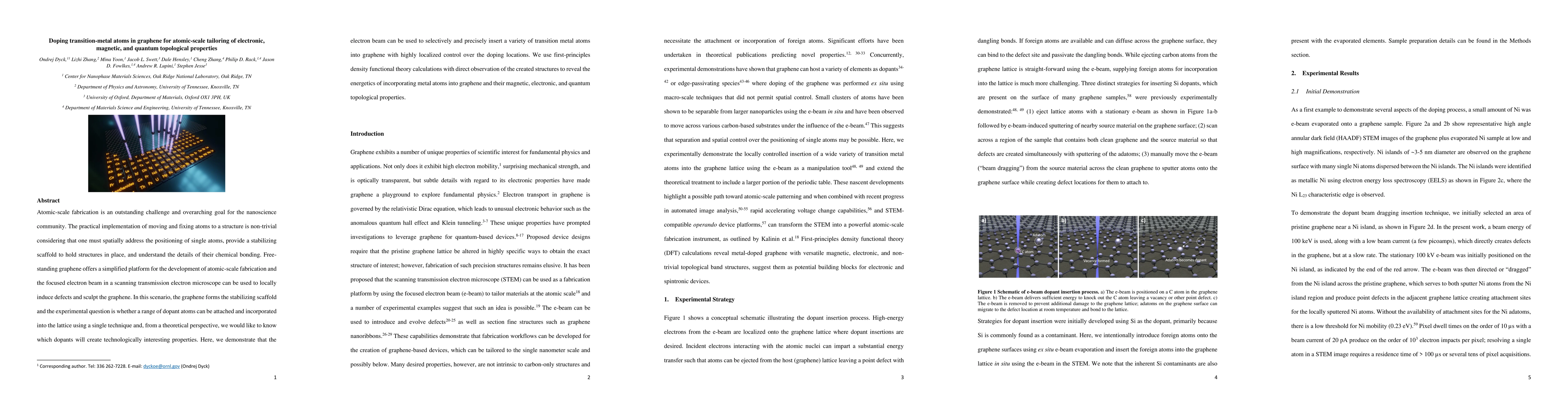
Atomic-scale fabrication is an outstanding challenge and overarching goal for the nanoscience community. The practical implementation of moving and fixing atoms to a structure is non-trivial conside...
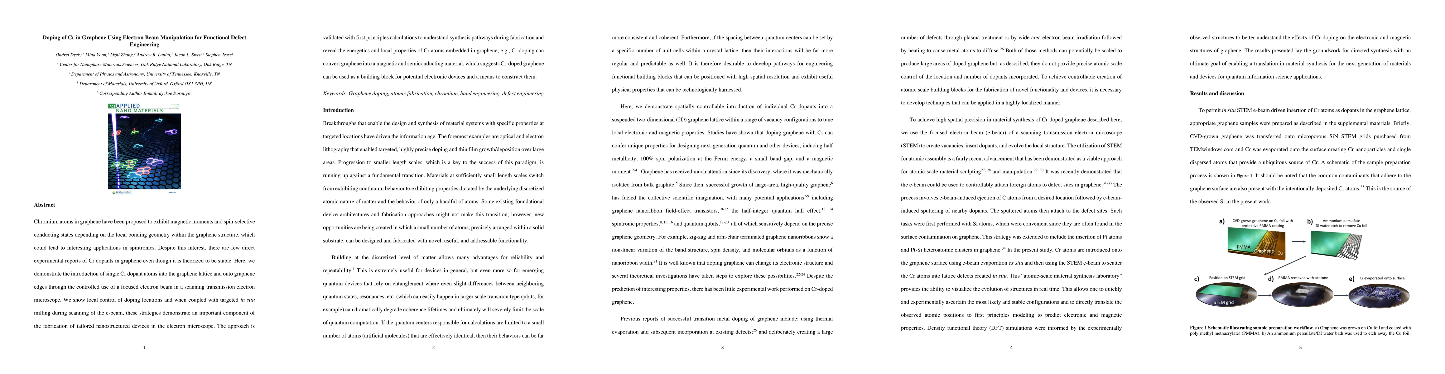
Chromium atoms in graphene have been proposed to exhibit magnetic moments and spin-selective conducting states depending on the local bonding geometry within the graphene structure, which could lead...

Graphene is of great scientific interest due to a variety of unique properties such as ballistic transport, spin selectivity, the quantum hall effect, and other quantum properties. Nanopatterning an...
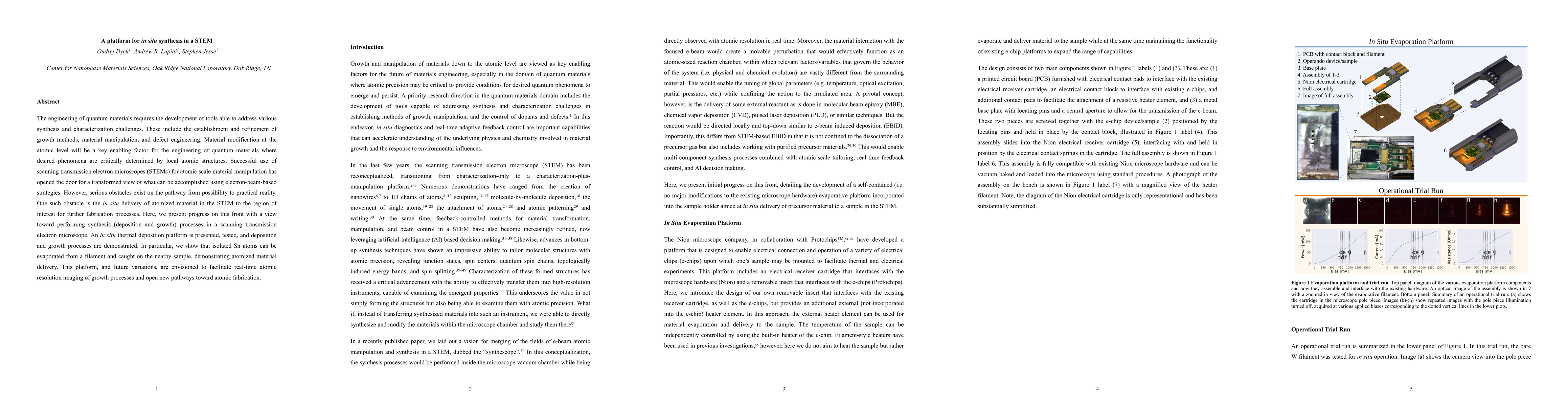
The engineering of quantum materials requires the development of tools able to address various synthesis and characterization challenges. These include the establishment and refinement of growth met...
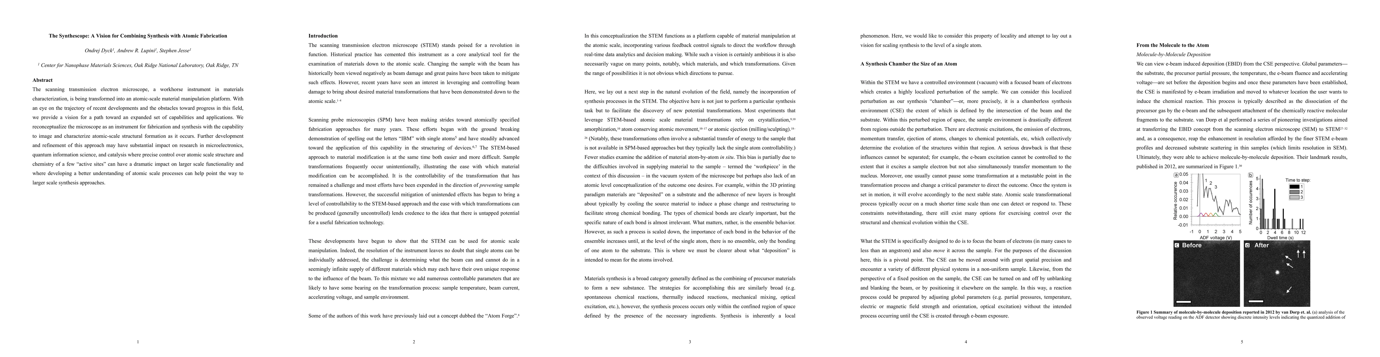
The scanning transmission electron microscope, a workhorse instrument in materials characterization, is being transformed into an atomic-scale material manipulation platform. With an eye on the traj...
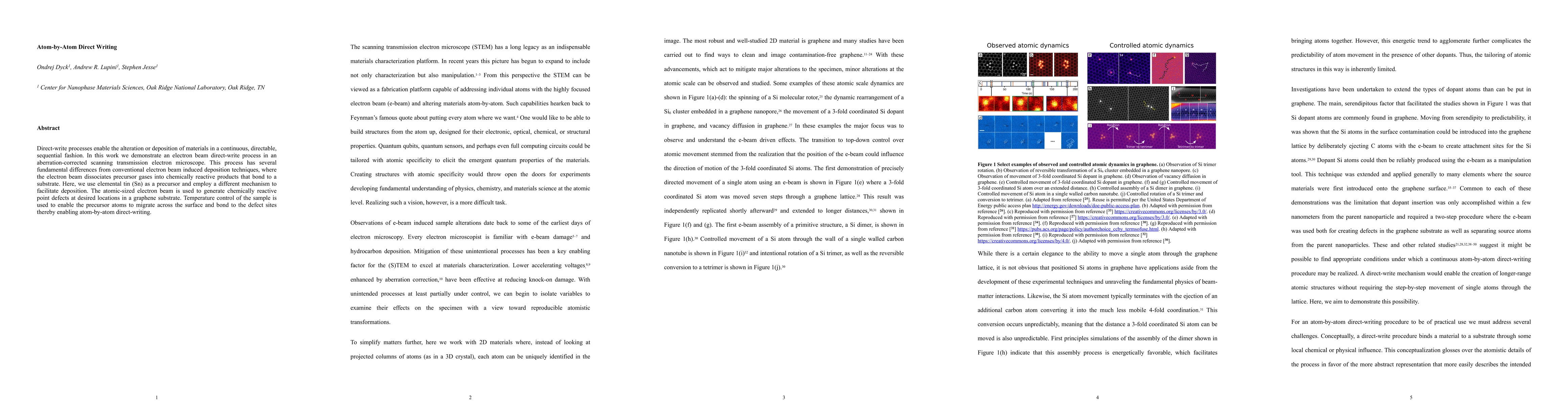
Direct-write processes enable the alteration or deposition of materials in a continuous, directable, sequential fashion. In this work we demonstrate an electron beam direct-write process in an aberr...
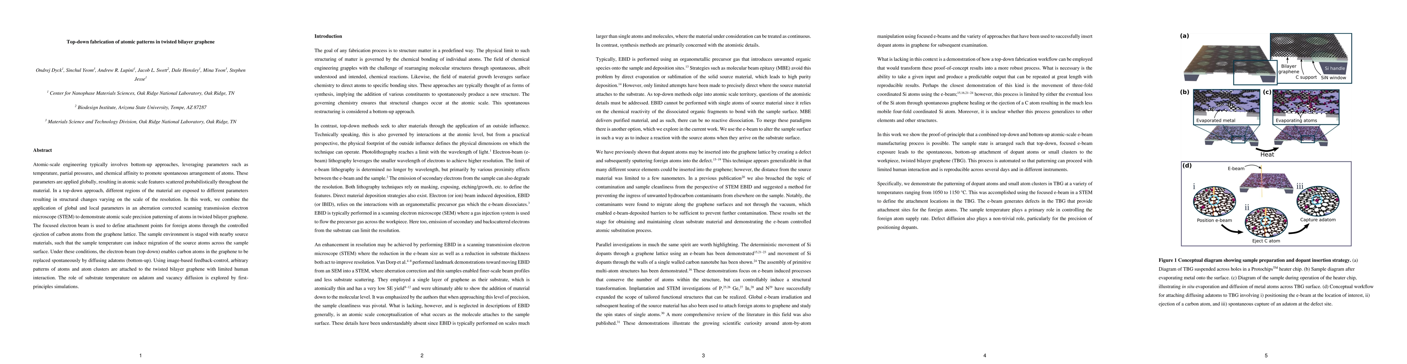
Atomic-scale engineering typically involves bottom-up approaches, leveraging parameters such as temperature, partial pressures, and chemical affinity to promote spontaneous arrangement of atoms. The...
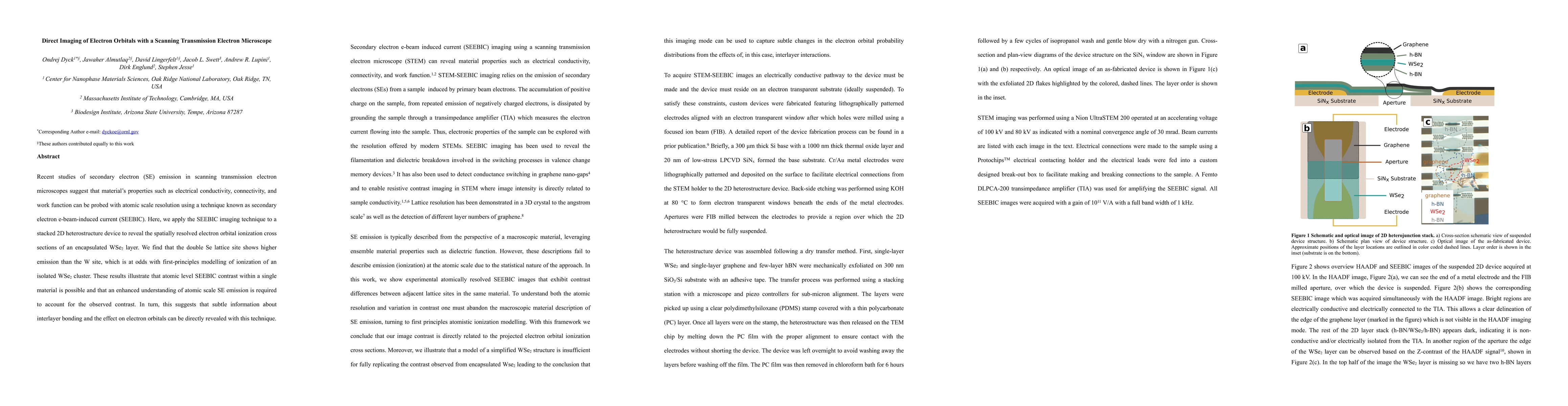
Recent studies of secondary electron (SE) emission in scanning transmission electron microscopes suggest that material's properties such as electrical conductivity, connectivity, and work function c...
The robust approach for real-time analysis of the scanning transmission electron microscopy (STEM) data streams, based on the ensemble learning and iterative training (ELIT) of deep convolutional ne...
Electron-beam (e-beam) manipulation of single dopant atoms in an aberration-corrected scanning transmission electron microscope is emerging as a method for directed atomic motion and atom-by-atom as...
Graphene has been proposed for use in various nanodevice designs, many of which harness emergent quantum properties for device functionality. However, visualization, measurement, and manipulation be...
Over the last few years, a new mode for imaging in the scanning transmission electron microscope (STEM) has gained attention as it permits the direct visualization of sample conductivity and electri...
Automated experiments in 4D Scanning Transmission Electron Microscopy are implemented for rapid discovery of local structures, symmetry-breaking distortions, and internal electric and magnetic field...
Recent advances in (scanning) transmission electron microscopy have enabled routine generation of large volumes of high-veracity structural data on 2D and 3D materials, naturally offering the challe...
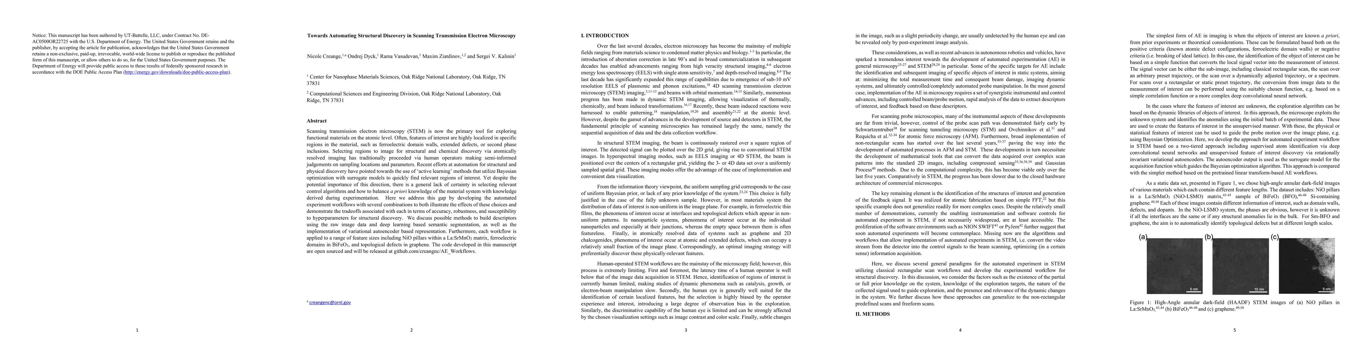
Scanning transmission electron microscopy (STEM) is now the primary tool for exploring functional materials on the atomic level. Often, features of interest are highly localized in specific regions ...
Research on two-dimensional materials has expanded over the past two decades to become a central theme in condensed matter research today. Significant advances have been made in the synthesis and su...
The 4D scanning transmission electron microscopy (STEM) method has enabled mapping of the structure and functionality of solids on the atomic scale, yielding information-rich data sets containing in...
The broad incorporation of microscopic methods is yielding a wealth of information on atomic and mesoscale dynamics of individual atoms, molecules, and particles on surfaces and in open volumes. Ana...
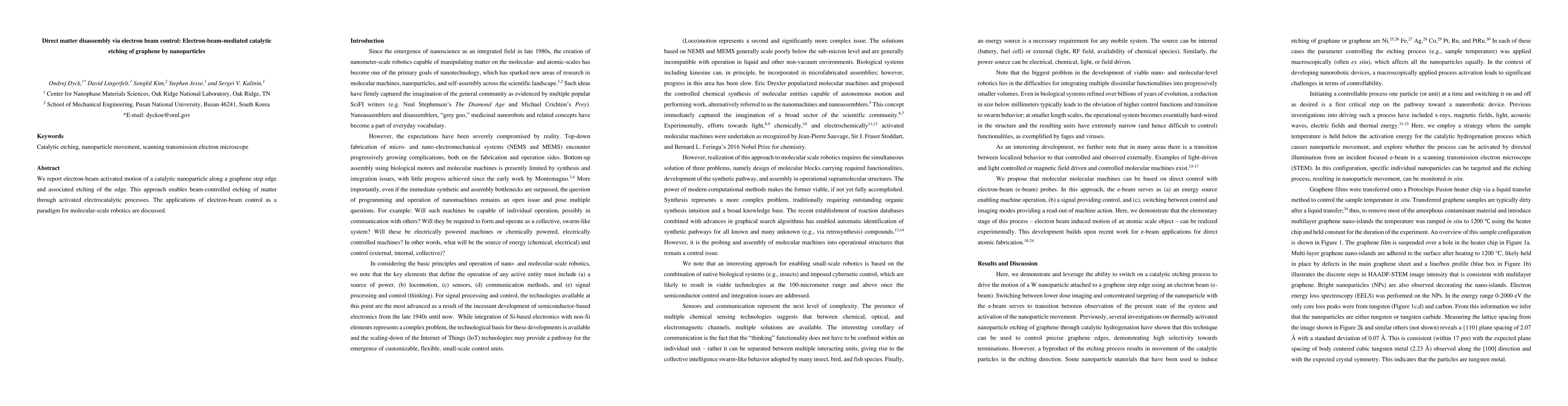
We report electron-beam activated motion of a catalytic nanoparticle along a graphene step edge and associated etching of the edge. This approach enables beam-controlled etching of matter through ac...
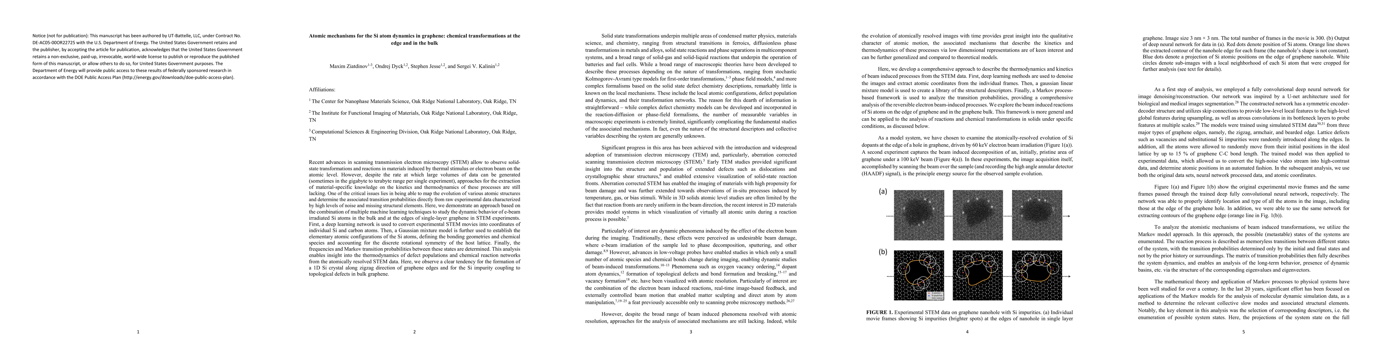
Recent advances in scanning transmission electron microscopy (STEM) allow to observe solid-state transformations and reactions in materials induced by thermal stimulus or electron beam on the atomic...
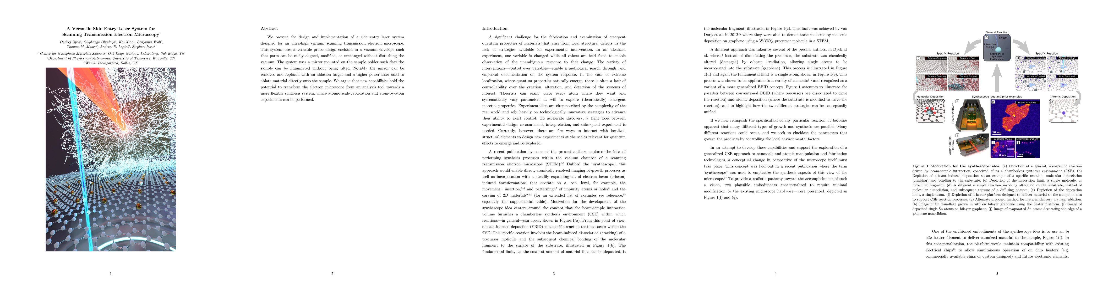
We present the design and implementation of a side entry laser system designed for an ultra-high vacuum scanning transmission electron microscope. This system uses a versatile probe design enclosed in...
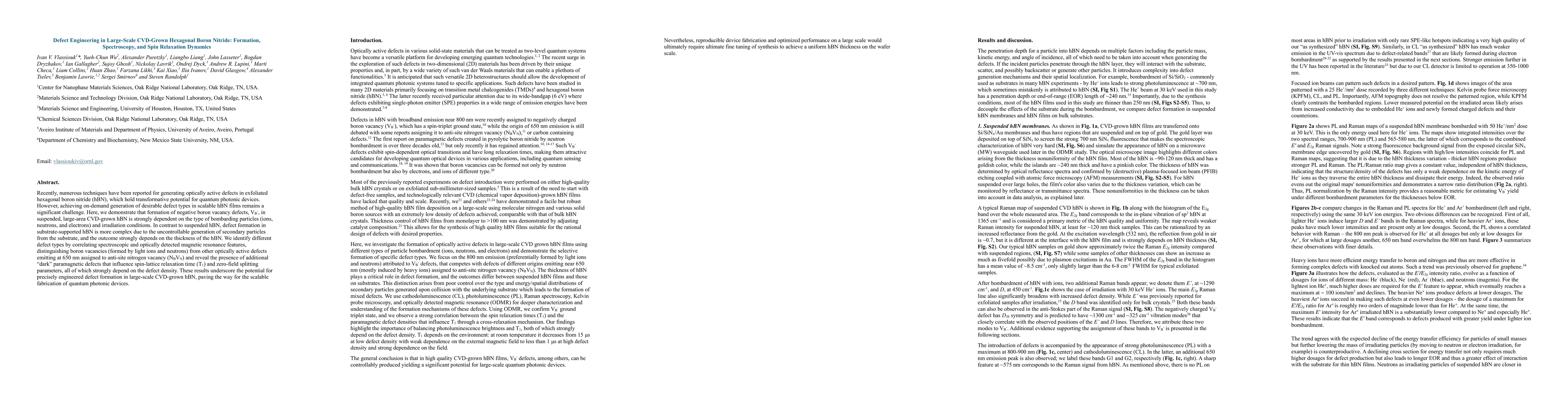
Recently, numerous techniques have been reported for generating optically active defects in exfoliated hexagonal boron nitride (hBN), which hold transformative potential for quantum photonic devices. ...
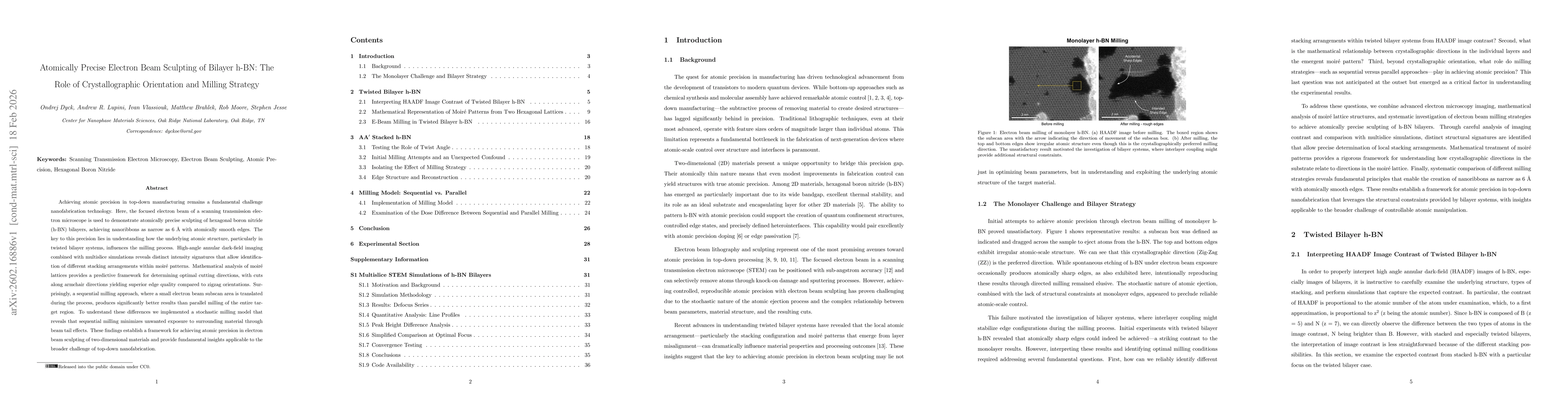
Achieving atomic precision in top-down manufacturing remains a fundamental challenge nanofabrication technology. Here, the focused electron beam of a scanning transmission electron microscope is used ...
Four-dimensional scanning transmission electron microscopy (4D-STEM) generates multi-gigabyte datasets, creating a growing mismatch between acquisition rates and practical storage, transfer, and inter...